
AD9833 Board
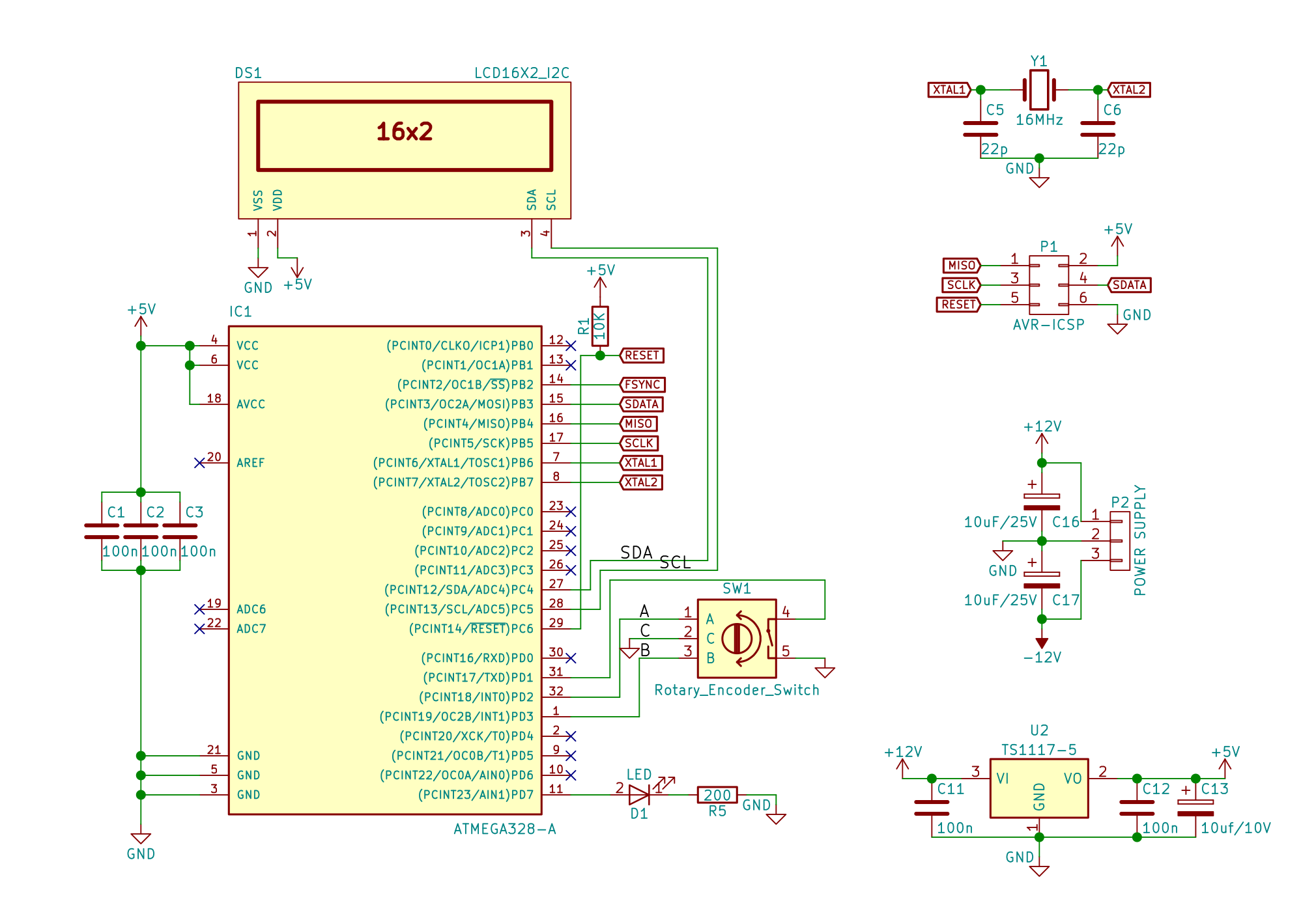
Let’s get to the main PCB. The LM1117-5V linear regulator is used to create a +5V rail from the +12V supply. To keep everything smooth, we add capacitors to both voltage input lines (+12V and -12V) and the output of the voltage regulator.
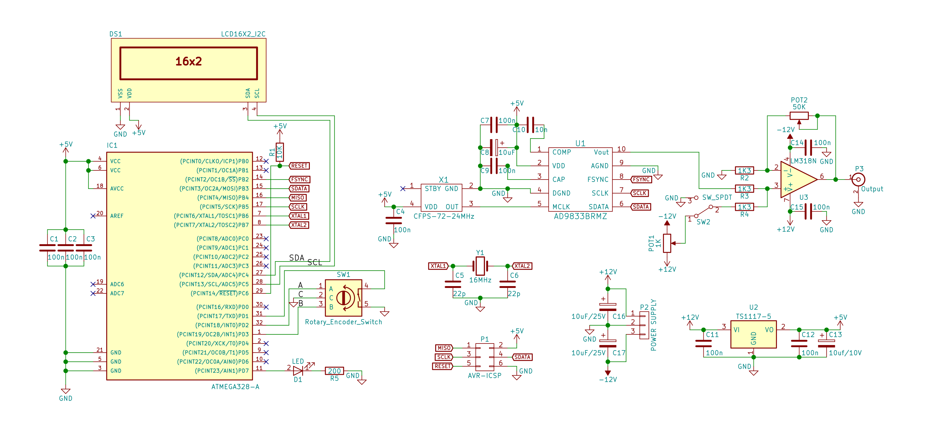
On the left side of the schematic, you will find an ATMega328p-AU microcontroller, the same used on the Arduino Uno but in an SMD package. To program the MCU, a 6-pin connector called AVR-ISP is placed next to it. It has two pins for power (+5V and GND) and four other pins for communication: MISO, MOSI, CLK, and RESET.
We will be using only one user input component, a rotary encoder with an integrated switch. This will be our control element to set the frequency, signal type, and other settings. The signals from the rotary encoder are routed to two interrupt pins on the microcontroller, PD2 and PD3 (D2 and D3 on the Uno), and the switch goes to an available pin that can act as an input; I chose PD1 (D1 on the Uno). We won’t be adding any pull-up resistors as we will be using the ones integrated into the microcontroller. Because mechanical contacts are not perfect, when we rotate the encoder, instead of an ideal pulse, a jittery signal will appear, but this can be easily fixed either by software or hardware using a capacitor. For the integrated switch, we will use the software method, and for the rotating contacts, two 100nF capacitors will be used.
A plain green LED is hooked up to pin PD7 (D7 on the Uno), for debugging purposes or to display status. The display used is a simple LCD with an HD44780 controller, which has 16 lines and two columns and includes a backlight. To reduce the number of connecting wires, an adapter board was used so that the only pins needed to control the LCD are 2 for data over I2C and another 2 for power (+5V and GND). The I2C lines on the microcontroller are on pins PC4 for SDA and PC5 for SCL. On the Arduino Uno, these are named A4 and A5, respectively.
Finally, the last connection for the microcontroller is made between it and the AD9833 integrated circuit. It uses a unidirectional SPI bus, meaning that data can only flow in one direction, from the MCU to the IC. The signals are MOSI (Master Out – Slave In), CLK (Clock), and CS (Chip Select, called FSYNC on the AD9833). To conclude the microcontroller portion, I should mention that decoupling capacitors with a value of 100nF are needed for each power supply pin.
Before continuing to the last part of the schematic, the part with the function generator IC, let me point out a few key features of the AD9833. Although I am going to sound like a salesperson, let’s start. It is a DDS type programmable waveform generator, so it takes a clock signal with a maximum frequency of 25MHz (for this particular IC), which it then divides based on a value passed by the microcontroller (maximum 228) via the SPI bus, and using a 10-bit DAC it outputs a waveform chosen by the microcontroller. The output has a peak-to-peak value of 0.65V-0.038V (VOUT maximum – VOUT minimum), and it has an offset of (0.65V-0.038V)/2. This means that VOUT minimum is very close to 0V. One important note is that the clock output (rectangular signal) has an amplitude of 2.5V, which is the voltage generated by the device’s internal voltage regulator.


