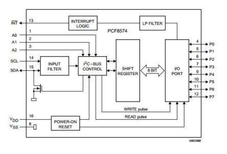
In this tutorial, I am going to show a I/O expander method using PCF8574A, which is a 8 bit I/O expander using I2C bus. This is another alternative other than using shift registers to expand either inputs or outputs such as 74HC595 (outputs) or 74HC165 (inputs). One of the advantages of using PCF8574A I/O expander is that it uses I2C bus, which requires only two data lines, they are clock (SCK) and data (SDA). Therefore, with these two lines, you can control up to eight of the same chip by changing the address input, providing extra 64 I/O pins.
Some of the features of PCF8574A IO Expander:
- Operating supply voltage 2.5V to 6V
- Open drain interrupt output
- I2C port to parallel port expander
- Address by 3 hardware address pins for use up to 8 devices (or even more, details will be covered later)
Obtained from PCF8574 Datasheet
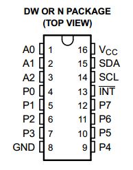
PCF8574A I/O expander is available in three different packages, namely Dual In-line Package (DIP16), Small Outline Package (SO16) and Shirnk Small Outline Package (SSOP20). I am going to use the DIP16 package since its easier for prototyping on breadboard.
The pinout diagram for PCF8574A is shown as image below.
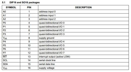
Pin explanation
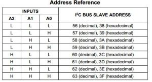
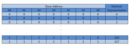
Pin 1,2 and 3 is used for hardware pin addressing. With three addressing pin, you can control up to eight of the same chip as mentioned previously. For example, you can connect all three pins to ground which makes the A2,A1,A0 to (000) while connecting pin 1 to HIGH and the other two to LOW will make A2,A1,A0 to (001) and so on. The address reference is shown as below.
Although I am using PCF8574A, there is another variant for this IC, which is PCF8574. The difference between these two ICs is the first four bit of address, for PCF8574 is 0100 whereas PCF8574A is 0111. Therefore, if you are using both of the ICs, you can expand to a maximum of 128 I/O ports.
Pin 4 to 7, 9 to 12 is the bidirectional input and output pins. You can configure these eight pins as either input or output pins.
Pin 13 is the open drain interrupt output. This can be used to inform the microcontroller if there is any incoming data on the ports.
Pin 14 and 15 is the I2C bus clock and data line. (Note that I2C data lines are open drain output). One of the advantages of using I2C bus for this chip is that you can control eight different ICs by manipulating pin 1,2,3, yet still using only two data lines. This is also the special features of I2C where you can control up to 128 devices on the same bus with 7 bit addressing.(If you not sure what I meant about the I2C addressing and the 128 devices , refer to the table below)
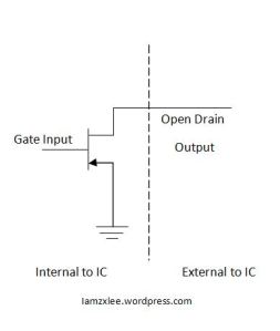
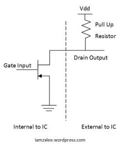
I have mentioned open drain output a few times during the pin explanation, so what does it really means? Open drain output means the line able to drive it’s output to LOW, but unable to drive it HIGH. In order to drive the output high, pull up resistor has to be connected at the drain output. Usually I will use 10k ohm resistor for pull up purpose on I2C bus. Even though you have multiple devices on I2C bus, you need only one pull up resistor on each line.
With a pull up resistor, when the gate input is LOW, the drain output is pull up to Vdd by the pull up resistor. Whenever the gate input is HIGH, the drain output will be connected to ground, implying a LOW on the output. The operation is similar to a resistive load MOS inverter.
So far I have covered the basics of the chip itself, let us focus on how to use the chip with Arduino. To interface PCF8574A using Arduino is easier with the Arduino built in library for I2c, <Wire.h>. This library will take care of the I2C protocol, so you don’t need too much of details to use I2C.
I am going to show two simple applications using PCF8574A. First, using PCF8574A as eight output pins and second, read inputs from PCF8574A and output from PCF8574A as well.
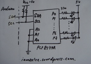
First, I will show how to set PCF8574A as output pins expander. The PCF8574A connections is shown as figure below. Eight LEDs are connected such that PCF8574A act as a current sink. In order to light up the LED, the output pin has to pull to ground.
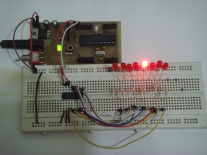
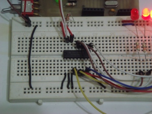
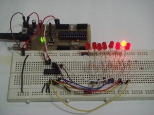
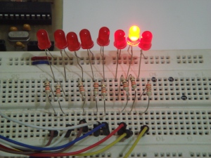
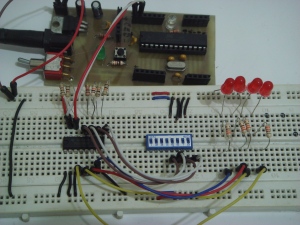
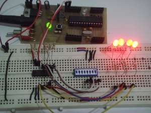
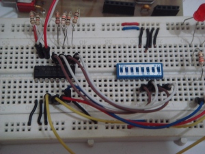
Some of the images of breadboard setup.
This is the code which I used to test the PCF8574A. The PCF8574A address is defined initially in the program. To output data to PCF8574A using Arduino, first, you need to begin the transmission to its address. Then write the desired output data. Finally, end the transmission to the address. Its quite easy to interface with PCF8574A to output data.
The program below will sweep through each output line of PCF8574A every loop. This is quite similar to a LED knight rider.
//coded by zxlee
//iamzxlee.wordpress.com

#include <Wire.h>

#define PCF_address B0111000 //A2 = A1 = A0 = 0

void setup()
{
Wire.begin();
}

void loop()
{
for(short temp=1;temp<=128;temp<<=1)
{
Wire.beginTransmission(PCF_address);
Wire.write(~temp);
Wire.endTransmission();
delay(500);
}
}
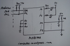
Next, I will show how to use PCF8574A as both input and output pins expander. Now, the lower nibble (P0 – P3) will be used as output pins to LEDs whereas the upper nibble (P4 – P7) will be used as input pins from DIP switches. Pull up resistor of 10k is used for each input line of DIP switch.
The program for PCF8574A is almost the same as being used as output pins. All you need to do is request data from PCF8574A, and read the data and store it in a variable. Then the data is used to control the output pins.
However, there is a little trick in reading data from PCF8574A. The input pins (P4-P7) cannot be pulled to ground. So in your program, you need to send HIGH to the input pins so that you can read from your switch. Refer to line 19 in the program below, where I pull the input lines to HIGH.
//coded by zxlee
//iamzxlee.wordpress.com

#include <Wire.h>

#define PCF_address B0111000

void setup()
{
Wire.begin();
Serial.begin(9600);
}

void loop()
{
byte temp=0;
Wire.requestFrom(PCF_address,1);
if(Wire.available())
temp=Wire.read();
Serial.print(temp);
Serial.print("t");
temp=(temp>>4)|0xF0;
Serial.println(temp);

Wire.beginTransmission(PCF_address);
Wire.write(temp);
Wire.endTransmission();

}
PCF8574A can be very useful especially when you are running out of I/O pins from Arduino. I have used it in my previous projects such as Digital Clock on 7 Segment Display for keypad and Wall Following Robot for LCD. In the future, I will show how to use PCF8574A for keypad and LCD.
