[tps_header][/tps_header]
Almost every smartphone uses a processor based on the ARM1 chip created in 1985.
The Visual ARM1 simulator shows what happens inside the ARM1 chip as it runs; the result (below) is fascinating but mysterious.[1]
In this article, I reverse engineer key parts of the chip and explain how they work, bridging the
gap between the puzzling flashing lines in the simulator and what the chip is actually doing.
I describethe overall structure of the chip and then descend to the individual transistors, showing how they are built out of silicon and work together to store and process data.
After reading this article, you can look at the chip’s circuits and understand the data they store.
Overview of the ARM1 chip
The ARM1 chip is built from functional blocks, each with a different purpose. Registers store data, the ALU (arithmetic-logic unit) performs simple arithmetic, instruction decoders determine how to handle each instruction, and so forth. Compared to most processors, the layout of the chip is simple, with each functional block clearly visible. (In comparison, the layout of chips such as the 6502 or Z-80 is highly hand-optimized to avoid any wasted space. In these chips, the functional blocks are squished together, making it harder to pick out the pieces.)
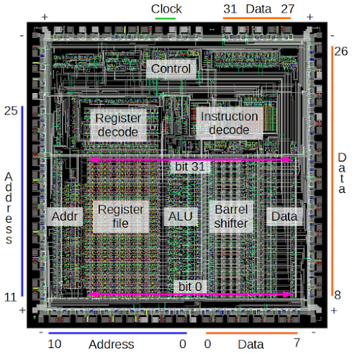
The diagram below shows the most important functional blocks of the ARM chip.[2]
The actual processing happens in the bottom half of the chip, which implements the data path. The chip operates on 32 bits at a time so it is structured as 32 horizontal layers: bit 31 at the top, down to bit 0 at the bottom. Several data buses run horizontally to connect different sections of the chip.
The large register file, with 25 registers, stands out in the image. The Program Counter (register 15) is on the left of the register file and register 0 is on the right.[3]
Computation takes place in the ALU (arithmetic-logic unit), which is to the right of the registers. The ALU performs 16
different operations (add, add with carry, subtract, logical AND, logical OR, etc.) It takes two 32-bit inputs and produces a 32-bit output. The ALU is described in detail here.[4]
To the right of the ALU is the 32-bit barrel shifter. This large component performs a binary shift or rotate operation on its input, and is described in more detail below.
At the left is the address circuitry which provides an address to memory through the address pins. At the right data circuitry reads and writes data values to memory.
Above the datapath circuitry is the control circuitry. The control lines run vertically from the control section to the data path circuits below. These signals select registers, tell the ALU what operation to perform, and so forth.
The instruction decode circuitry processes each instruction and generates the necessary control signals. The register decode block processes the register select bits in an instruction and generates the control signals to select the desired registers.[5]


