
Now that we have got that out of the way, let’s look at the last part of the schematic. A crystal oscillator is used to feed a 24MHz clock signal to the master clock input of the AD9833. FSYNC, SCLK, and SDATA are connected to the SPI bus of the microcontroller. Two decoupling capacitors are used near the VDD pin, one with a value of 0.1µF and another one with a value of 10µF. Another decoupling capacitor is needed for the 2.5V internal voltage regulator; this is near the pin CAP and has a value of 0.1µF. One more capacitor is needed between the COMP and VDD pins for decoupling the DAC bias voltage; it has a value of 10nF, as indicated by the datasheet.
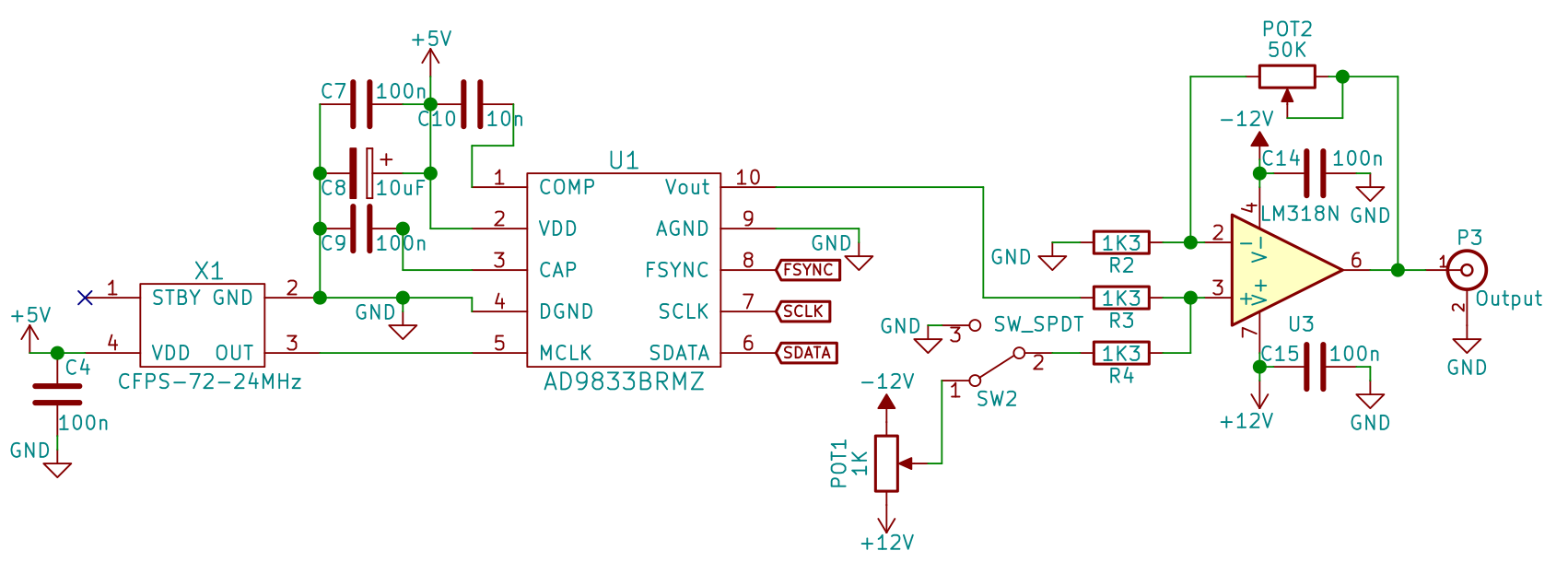
A few paragraphs above when I was talking about the microcontroller connections, I also wrote the Arduino Uno pin equivalents. I did this because the AD9833 circuit described in the previous paragraph is available at various Chinese manufacturers as a breakout board that you can connect to an Arduino Uno. Keep in mind that the output is straight from the IC, without the additional circuitry that I will continue to explain below.
The output of the IC is fed into the non-inverting input of the op-amp using a 1.3kΩ resistor. The trimmer POT1 (a variable resistor), which has its side pins connected to -12V and +12V, has the sweeper connected to a switch’s input terminal to provide an offset voltage. The other input terminal of the SPDT switch is wired directly to ground, and the output terminal is connected to the non-inverting input of the op-amp with another 1.3kΩ resistor. This configuration combined with a 50kΩ potentiometer allows us to have a variable gain between 1 and approximately 20. This was computed using Millman’s theorem and the fact that the op-amp keeps its inputs, V+ and V-, at the same voltage:
V+=VinR3+VoffsetR41R3+1R4V+=VinR3+VoffsetR41R3+1R4
V−=VoutPOT21POT2+1R2V−=VoutPOT21POT2+1R2
V+=V−V+=V−
Vout≈20Vout≈20
Keep in mind that the gain is also applied to the offset voltage. I did this to have three configurations:
- The offset voltage is set to -350mV using the trimmer POT1. When the switch is in position 3 (R4 connected to ground), the output voltage is the output of the IC, a signal with an amplitude of 350mV and an offset of 350mV, multiplied by the gain set by the potentiometer POT2. When the switch is in position 1 (R4 connected to the offset voltage obtained by the trimmer POT1), the output is just as before minus the offset voltage, essentially a signal with a 350mV amplitude and no offset, multiplied by the gain.
With this configuration, the output voltage can either swing from -7V to +7V or from 0V to what the op-amp is capable of (something near +12V). - The offset voltage is set to VOUT minimum of the AD9833. This is then multiplied by the gain, which can vary from 1 to 20.
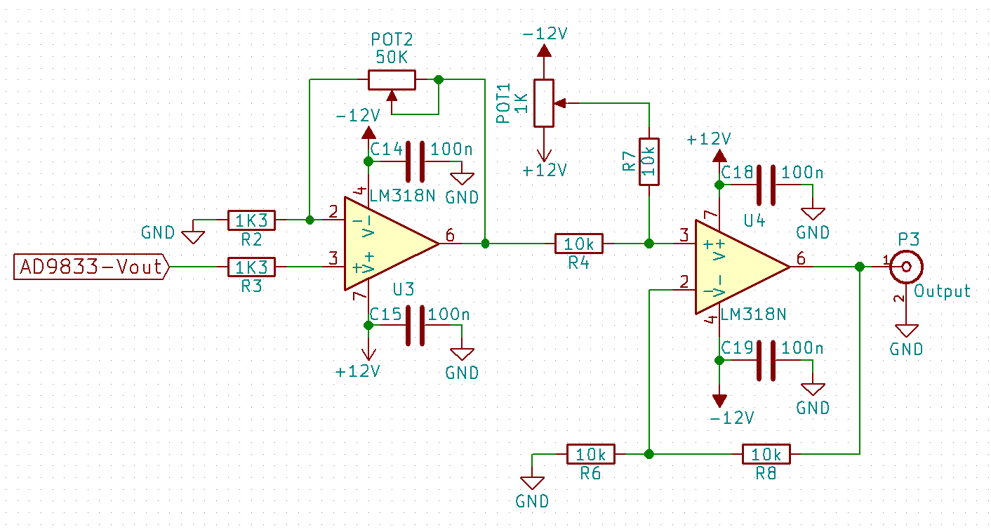
- Instead of the trimmer POT1, you can use a potentiometer and mount it on the front panel so you can have a variable offset. Just remember that the offset is also affected by gain, so it is wise to first set the gain, to choose the peak-to-peak voltage that you need, and after that use the offset potentiometer to adjust the signal’s vertical position. I do not recommend this setup; if you want variable offset, I suggest that you add a separate op-amp as a summing amplifier with a fixed gain of 2, as in the schematic below.
Vout=40⋅Vin+VoffsetVout=40⋅Vin+Voffset
In order to wrap up the amplifying part of the circuit, I have to mention that you will need 100nF decoupling capacitors for both the positive and the negative power supply and that you need to choose an op-amp that can withstand the power supply voltages (+12V and -12V) and that has a very good slew rate, so that it can keep up with high-amplification signals.


