
The relationship connecting current and voltage at the inductor’s ends is the following one:
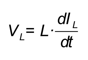
that indicates that the voltage at the inductor’s ends is equal to its value, multiplied for the variation of the current in time.
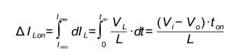
By inverting and integrating the equation, it is possible to obtain the period in which the switch is closed:
And as for the period in which the switch is open:

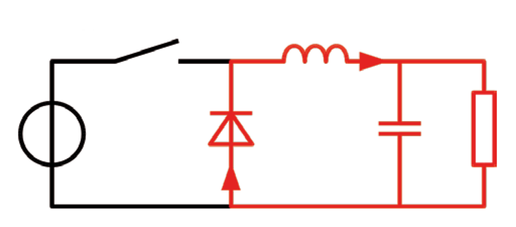
From these two equations it is possible to notice that, during the switch’s closing time, the inductor’s current grows proportionally to the difference between the input voltage and the output voltage (Vi-Vo) and to the switch’s closing time and inversely with respect to the inductance value.
With a simplification, the greater the difference between Vi and Vo and the closing time, the smaller is the inductance, the more the current grows in output.
During the switch’s opening time, on the other hand, the inductor is unloaded (with a minus sign before Vo in the equation) in a proportional way with respect to the output voltage, and inversely with respect to the inductance value. An aspect that quickly stands out is that the greater the inductance and the less the current growing in the coil, which is translated in less “efforts” in the circuits that surround it, but to a big inductor correspond greater dimensions and/or greater losses due to the electrical resistance of the wire with which it is built (we will talk about this later).
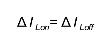
Having considered the hypothesis of a stationary regime, that is to say with constant output voltage and current in the inductor that is never null, we will see that the current accumulated during the switch’s closing will have to be released exactly and entirely during the switch’s opening; therefore we may write that:
That is to say, by substituting with what has been obtained before:

Since we are interested in calculating the output voltage value on the basis of the switch’s closing and opening times, we will solve for Vo :
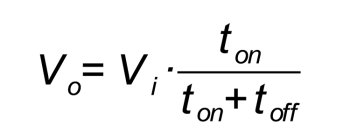
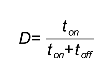
And, by naming D the switch’s duty-cycle (that is to say, the ratio between the time in which it remains closed and the total time):
We may write down the final equation of our converter:

Please notice that the D duty-cycle may have values ranging between 0 and 1, therefore the output voltage may be lower or equal to the input one, but never greater, with this type of converter.
For those who know a bit about Arduino world and its PWM outputs, it is easy to think to use a MOSFET in the place of the switch, and to apply a square wave supplied by one of Arduino’s outputs to the gate. For example, by choosing a 25% value for D, we will obtain a quarter of the input voltage as an output.
Someone will have noticed that in our very beautiful and simple equation the inductance, L, has disappeared and therefore it doesn’t influence the output voltage value in any way.
We may therefore choose any value for L? In theory, yes, if we weren’t interested in other factors and, above all, if the inductor was an ideal one, that is to say, without any electrical resistance in the wire composing it.
We already saw before, in fact, that the current in the inductor (and therefore in a great part of the circuit) grows faster with the decrease of the inductance itself and with the increase of the closing time.
Therefore, with low inductance values and/or with long switch’s closing times, the current will grow a lot, with the risk to damage the same components; moreover, great variations in the current correspond to great electromagnetic disturbances, that are generated by the circuit and that end in the powered device.
In contrast, if we increase the inductance too much, it will have a quite high resistance due to the wire (the higher the value, the more wire coils are needed), which will determine losses of the energy that is transformed in heat, and a consequent loss of efficiency of the converter, in addition to a greater size.
Moreover, it is possible to notice that, with all other things being equal (inductance and Vi and Vo values), by decreasing the closing and opening times, the current is kept lower. A decrease in the opening and closing times (when keeping D constant) however corresponds to an increase in the switching frequency; it would be best, therefore, to choose a small inductance and a frequency being the highest as possible.
Unfortunately, even if we are trying to do everything possible by taking advantage of the modern electronic components, there are some impassable limits, both for the frequency with which the same may operate, and for the switching losses, due to the fact that an instant action is impossible.
Even here a compromise between the high frequency and the possibilities given by the components available is necessary; if for a converter having discrete components it was already something extraordinary to reach and exceed a frequency of a few hundreds of kHz, with the modern integrated circuits it is possible to reach frequencies that are greater than a MHz and, in the last years, even greater than 3 MHz.
This is translated in a greater compactness of the power supplies, a greater efficiency and a lesser cost, at the price of a greater attention needed when disposing the components on the PCB, as we will see in the second installment, in which we will present a practical converter circuit.


