
By opening the switch we reach the situation depicted in figure: since the L1 inductor makes it impossible to have an instant variation of the current, all the current flowing through L1 will have to forcedly flow through C1 as well. The current in L2 will continue flowing as before in the opposite direction, but this time it will flow through the load (red line in the diagram shown in figure). We will see therefore a negative current (IL1) that will be added to the IL2 current.
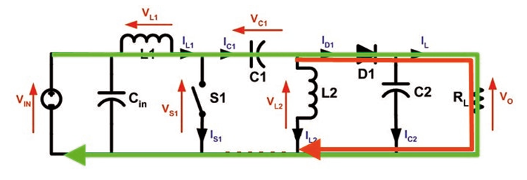
From Kirchhoff’s Law, applied to the nodes, we obtain the following relationship:
ID1 = IC1 – IL2
therefore the current at the load, with the switch open, is supplied by both L2 and L1, while the C1 capacitor is recharged by L1.
In summary:
- with the switch closed, the power source charges L1, while C1 charges L2;
- with the switch open, the L1 and L2 inductors power the load, while L1 recharges C1.
During the operations, the voltage on C1 may change its sign , therefore we need to insert another component: a non polarized capacitor.
The converter’s functioning may be seen as the coupling of a boost converter, composed of L1 and the switch, that generate a VS1 voltage that is greater than the one of the power source; it is followed by a buck converter that reduces VS1 to the required value.
Since the voltage at C1’s ends is equal to VIN, as previously seen, the output voltage becomes:
VO = VS1 – VIN
Therefore if VS1 is less than twice the amount of VIN the output voltage will be lower than the input one, in the opposite case it will be greater.
Without going further into detail, the equation regulating the relationship between input and output voltage is equal to:
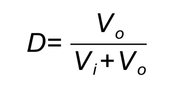
in which D represents the usual duty-cycle, that is to say the ratio between the times of the switch being closed and the total time (open + closed switch).
From here it is possible to extract:
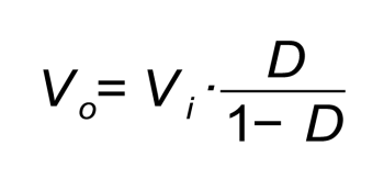
That shows how the output voltage is lower than the input one with D < 0.5 and it is greater with D > 0.5.
The abovesaid formulae are true, as usual, in the absence of dissipating (resistive) components and/or non linear ones (MOSFETs, diodes, etc.) in the circuit, which is something that is not true, in practice; for example, we have to consider the voltage drop on the diode, the coils resistances, the capacitor’s ESR, etc., that contribute both to slightly modify the formula and to decrease the efficiency.
Originally published at Open Electronics.
[tps_footer][/tps_footer]


