
Quick Answer
Driving a MOSFET gate means moving charge into and out of a capacitor, not holding a voltage on a terminal. How quickly that charge moves sets how long the device spends between its two states, and the device dissipates far more during those crossings than in either state.
Intuition
A bucket, not a wire
Ask what voltage a MOSFET gate needs and you get a useful answer. Ask how much current it needs and the honest reply is: in the steady state, none at all. The gate is insulated from everything else in the device. Once it is charged it stays charged, and holding it there costs nothing.
That makes it sound easy, and it hides the actual problem. Getting to that state means filling a bucket, and the bucket has to be filled before the device changes what it is doing. A gate is a charge input. The datasheet parameter that matters is not a voltage but a quantity of charge in nanocoulombs, and the time it takes to deliver that charge is the time the device spends being neither on nor off.
Being neither on nor off is expensive. On, a MOSFET has voltage across it and almost no current. Off, it has current through it and almost no voltage. In between, it briefly has both at once, and the product of two large numbers is a large number.
The whole subject is that in-between. How to make it short, what making it short costs, and why past a certain switching frequency it becomes the only loss worth talking about.
Practitioner
What the gate actually asks for
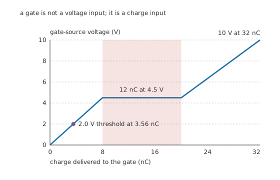
A gate is not a voltage input; it is a charge input.
Plot the gate's voltage not against time but against the charge that has gone into it, and the device tells you its whole story in three straight lines.
Worked example — Reading the three segments
The first rise. The gate charges like an ordinary capacitor. 8.0 nC takes it to 4.5 V, crossing the 2.0 V threshold on the way at 3.56 nC. Somewhere in here the device starts conducting.
The flat part. Then 12 nC goes in and the gate voltage does not move at all. This is the Miller plateau, and it is where the drain voltage is doing its swinging.
The second rise. A further 12 nC takes the gate up to the full 10 V — 32 nC in total — and buys the low on-resistance that a hard drive is for.
The plateau is the interesting one, because it is charge that produces no change in gate voltage and all of the change in drain voltage. Its length in time is the switching time.
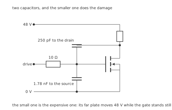
Two capacitors, and the smaller one does the damage.
The plateau exists because the gate is not only coupled to the source. There is a second, much smaller capacitance from the gate to the drain — and the drain is the terminal that swings.
Worked example — Why the small capacitor costs the most
The two capacitances follow from the charges. 1.78 nF sits between gate and source, charged across the 4.5 V the plateau sits at. 250 pF sits between gate and drain — seven times smaller — but it is charged across the drain's whole 48 V swing.
Small capacitance, large swing, and the charge is the product: 12 nC, more than the whole first segment.
While that charge is moving, the gate is held still. The driver's current is going entirely into the gate-drain capacitor rather than raising the gate, because the far plate is falling as fast as the near plate would rise. The gate voltage is pinned, and it stays pinned until the drain has finished moving.
That is why the plateau charge, not the total, is what sets switching speed. A part with a large total gate charge but a small gate-drain charge switches faster than its headline number suggests, and the reverse is also true.
Engineer
The crossing, and what it costs
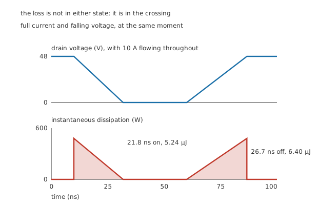
The loss is not in either state; it is in the crossing.
Follow one cycle with the load current flowing the whole time — the standard hard-switching picture, and a deliberately pessimistic one, since it assumes the current is at full value across both edges.
Worked example — One transition, in joules
The driver has 10 V to give and the gate is pinned at 4.5 V, so 10 Ω passes 550 mA. Moving 12 nC at that rate takes 21.8 ns.
Turning off is slower, because the driver is pulling the gate down from 4.5 V to ground rather than up from it: 450 mA, so 26.7 ns. Together, 48.5 ns of crossing per cycle.
During each crossing the device holds a falling voltage while passing 10 A. At the start of the turn-on edge that product is 480 W — instantaneously, in a package rated for a few watts.
It falls linearly to zero, so the energy is half the peak times the width: 5.24 µJ turning on and 6.40 µJ turning off, 11.6 µJ per cycle.
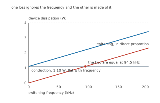
One loss ignores the frequency and the other is made of it.
Eleven microjoules sounds like nothing. It is nothing — once. The number that matters is how often.
Worked example — Where the two losses meet
Conduction loss does not care about frequency at all. At 10 A through 22 mΩ for 50 % of the time, it is 1.10 W whether the device switches once a second or a million times.
Switching loss is 11.6 µJ multiplied by the frequency — a bare proportionality through zero. At 100 kHz it is 1.16 W.
The two are equal at 94.5 kHz. Below that the device's resistance is the thing to improve; above it, nothing about the resistance matters much and the transitions are the whole problem.
Every switching converter's frequency choice is an argument with this graph. Higher frequency means smaller inductors and capacitors, and it means paying for every transition more often.
Professional
One resistor, two bills
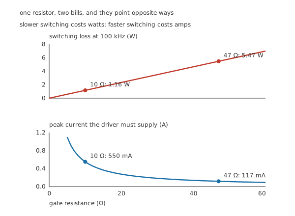
Slower switching costs watts; faster switching costs amps.
The gate resistor looks like the least consequential component on the schematic. It sets both of the numbers this lesson is about, and it sets them in opposite directions.
Worked example — Ten ohms against forty-seven
Every plateau current goes inversely with the gate resistance, so every switching time goes in direct proportion to it, and so does the loss.
At 10 Ω, the crossing takes 48.5 ns and costs 1.16 W at 100 kHz. At 47 Ω it takes 228 ns and costs 5.47 W — 4.7 times as much, from one component change.
The bill going the other way is peak current. The driver must supply 550 mA with the smaller resistor and only 117 mA with the larger one.
So a small gate resistor demands a driver that can source and sink hundreds of milliamps in nanoseconds — which is exactly what a dedicated gate-driver chip is for, and why a microcontroller pin is not one.
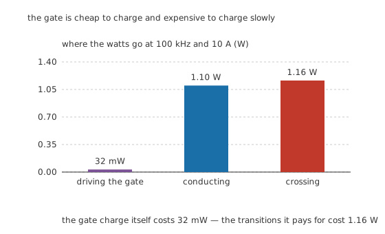
The gate is cheap to charge and expensive to charge slowly.
Worked example — The three bills, side by side
Driving the gate costs 32 nC at 10 V, delivered 100 kHz times a second: 32 mW. All of it is dissipated in the driver and the gate resistor rather than in the device.
Conducting costs 1.10 W.
Crossing costs 1.16 W.
The gate charge itself is thirty-odd times smaller than the loss it controls. That is the shape of the whole subject: the cheapest thing on the list decides the size of the two expensive ones, so it is worth spending on a driver that delivers it quickly.
Four things that follow
Gate drivers exist for four reasons, not one. Peak current is the obvious one. The others are level shifting for high-side devices, whose gates are referenced to a moving source; separate turn-on and turn-off paths, so the two edges can be set independently; and under-voltage lockout, which holds the gate down rather than half-driving a device through a supply dip.
Layout is part of the drive circuit. The loop from the driver's output, through the gate resistor, into the gate and back through the source carries hundreds of milliamps with nanosecond edges. Its inductance is in series with everything this lesson computed, and a centimetre of extra track can ring the gate hard enough to produce a second, unwanted turn-on.
A falling drain can turn a device on through its own feedback capacitance. The same gate-drain capacitor that makes the plateau will inject current into the gate when the drain moves quickly — which in a bridge leg is exactly when the other device is switching. A low-impedance path from gate to source, or a negative off-state gate voltage, is the standard defence, and it is one reason a large gate resistor can be actively dangerous rather than merely wasteful.
Soft switching changes the shape of the argument. Circuits that arrange for the voltage to be near zero when the device turns on, or the current to be near zero when it turns off, shrink the crossing triangles rather than shortening them. The reasoning is the same and the answer is different, which is why resonant converters can switch at frequencies that would destroy the hard-switched circuit computed here.
Common mistakes
- Treating the gate as a voltage input — it is a charge input. What the device costs to switch follows from 32 nC and how fast it is delivered, not from the 10 V it ends at.
- Sizing the driver from the average gate power — 32 mW is genuinely nothing, but it arrives in 550 mA bursts a few tens of nanoseconds long. The driver is specified by the peak, not the average.
- Reaching for a large gate resistor to be gentle — 47 Ω instead of 10 Ω multiplies the switching loss by 4.7, and a slowly-driven gate is more vulnerable to being turned on by its own drain.
- Judging switching speed by the total gate charge — the plateau charge is what sets it: 12 nC of the 32 nC here. A part with a large total but a small plateau charge switches faster.
- Ignoring frequency when choosing a device — below 94.5 kHz the on-resistance is what to improve; above it, the transitions dominate and a lower-charge device beats a lower-resistance one.
- Driving a power MOSFET straight from a logic pin — a pin that can source a few milliamps will take microseconds over a transition that should take tens of nanoseconds, and the device will be in its crossing region for most of every cycle.
Frequently asked questions
If the gate draws no steady current, why does gate drive matter?
Because getting to the steady state means delivering charge — 32 nC here — and the device is in its lossy in-between region until that charge has moved. Holding the gate costs nothing; changing it costs the switching loss, which at 100 kHz is 1.16 W against 32 mW of gate power.
What causes the Miller plateau?
The capacitance from gate to drain. While the drain swings, the driver's current goes entirely into charging that capacitor rather than raising the gate, so the gate voltage sits still at 4.5 V until the drain has finished moving. Here that means 12 nC delivered with no change in gate voltage at all.
How do I choose the gate resistor?
By deciding which bill you would rather pay. Switching loss is in direct proportion to it — 1.16 W at 10 Ω and 5.47 W at 47 Ω — and the peak current the driver must supply goes inversely, 550 mA against 117 mA. Small enough that the loss is acceptable, large enough that the driver and the layout can supply the current cleanly.
Why is turning off slower than turning on?
Because the driving voltage across the gate resistor is different in each direction. Turning on, the driver has 10 V pushing against a gate pinned at 4.5 V, so 550 mA flows. Turning off, only the 4.5 V on the gate itself drives the discharge, so 450 mA flows and the same 12 nC takes 26.7 ns rather than 21.8 ns.
At what frequency does switching loss start to matter?
Where it equals the conduction loss, which for this device and this load is 94.5 kHz. Below that, a lower on-resistance is the useful improvement. Above it, a lower gate charge is, and the two are rarely available in the same part.