
Quick Answer
The Hall effect is the appearance of a voltage across a current-carrying conductor when a magnetic field passes through it. The field pushes the moving charge carriers to one side until the voltage they build up balances that push. Its size depends on the material, which is why Hall sensors use semiconductors.
Intuition
Reading a current without touching the wire
A clamp meter that measures alternating current can be a coil and nothing else, because an alternating current makes a changing field and a changing field makes a voltage in a coil. Ask that same meter to read the direct current from a battery and it goes blank. The field is there, steady and perfectly measurable, but a coil only responds to change, and nothing is changing.
The instrument that fills that gap does something different. It puts a thin sliver of semiconductor into the field, passes a small current along it, and reads a voltage that appears across the sliver, at right angles to both. That voltage is proportional to the field and it does not care whether the field is steady. Edwin Hall found the effect in 1879, and for a century it was mostly a laboratory curiosity for measuring what materials are made of.
What changed is that the same sliver turned out to be an ideal magnetic sensor. It has no moving parts, it works down to zero frequency, it costs very little, and it can be built on the same silicon as the amplifier that reads it. Hall devices now sit inside DC clamp meters, motor controllers that need to know where the rotor is, contactless switches, and the current-sensing loop of most things that charge a battery.
Practitioner
The sideways voltage, and what sets its size
Drive a current along a flat plate and put a field through the plate's face. The moving carriers are pushed sideways, they pile up along one edge, and the charge separation builds a voltage — until that voltage pushes back hard enough to cancel the sideways force. The plate settles there, and the voltage it settles at is the Hall voltage.
The Hall coefficient R_H is the material's contribution, and thickness appears in the denominator because a thinner plate crowds the same current into a smaller cross-section.
Worked example — A doped-silicon Hall plate
A plate of Hall coefficient 0.000625 cubic metres per coulomb, 50 µm thick, carrying 10 mA in a field of 100 mT, develops 12.5 mV across its edges.
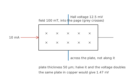
Three properties of that relationship do the practical work. It is linear in the field, so a Hall device makes a well-behaved analogue sensor rather than a threshold detector. It is linear in the drive current, which means the output is proportional to the product of two inputs — the basis of Hall-effect multipliers and wattmeters. And it reverses sign with the field, so a Hall sensor distinguishes a north pole from a south pole, which a coil-based sensor at rest cannot do at all.
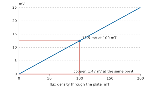
Twelve millivolts from a hundred millitesla is small but entirely workable, and it is the reason a modern Hall sensor arrives as a three-terminal device with the amplifier already inside it rather than as a bare plate.
The drive current is a design variable rather than a constant of nature, and raising it raises the output in proportion — up to the point where the plate's own dissipation starts heating it, which shifts both the sensitivity and the offset. Integrated devices settle that trade internally and present you with a supply pin instead, which is why a datasheet quotes sensitivity in volts per tesla rather than the raw Hall coefficient. Where you do meet a bare element, in a laboratory gaussmeter probe, the drive current is specified alongside the calibration and changing it invalidates both.
One point of vocabulary saves confusion later. What the plate responds to is flux density at its own face, in tesla, not the total flux through some larger area. A Hall device is a point sensor, and putting it in a wider gap does not average the field across that gap; it reads whatever is happening in the few square millimetres it occupies, which is why the mechanical placement of a current sensor in its core matters as much as the core does.
Engineer
Why the plate has to be a semiconductor
The Hall coefficient is not an arbitrary material property. It is the reciprocal of the carrier density multiplied by the carrier charge, so a material with few carriers has a large coefficient, and one with many has a small one. Metals conduct well precisely because they have enormous carrier densities, and that is exactly what ruins them as Hall elements.
Worked example — The same plate, in copper
Copper's Hall coefficient is 0.0000000000734 cubic metres per coulomb — written out in full, because that string of zeros is the result worth seeing. The identical plate, same current, same field, gives 1.47 nV.
The doped-silicon version is larger by a factor of 8.5 M.
That figure is the free-electron-model value, the textbook estimate for a metal with one conduction electron per atom. The measured coefficient is closer to −5.3×10⁻¹¹ m³/C — smaller in magnitude, and negative, the sign a direct signature of electrons rather than holes doing the conducting. Either number makes the same point: copper's coefficient is minuscule next to doped silicon's.
A nanovolt and a half is below the noise of any practical amplifier and drifts with temperature by more than its own value. Doped silicon and the compound semiconductors used for the best devices have carrier densities millions of times lower, and they buy their sensitivity with exactly that scarcity. This is the same trade a semiconductor's doping level always represents: a controllable, deliberately small population of carriers is worth far more than a large uncontrollable one.
The sign of the Hall voltage carries information too. It tells you whether the carriers doing the conducting are negative or positive, and in a p-type semiconductor the answer really is positive — holes. That measurement was one of the earliest hard confirmations that hole conduction is not merely a bookkeeping convention, and it is still how carrier type and concentration are measured in a fabrication line.
Geometry limits the model in a way the expression does not admit. It assumes a plate much wider than it is thick and much longer than it is wide, so that the current is uniform and the drive contacts sit far from the sensing ones; a squat element short-circuits part of the Hall voltage back through its own drive contacts and gives measurably less than the relationship predicts. Manufacturers quote a geometric correction factor for exactly this reason, and it is one of the things you are paying for when you buy a device rather than etching a plate.
Orientation limits it too. The relationship counts only the field component perpendicular to the plate's face, so a tilted field contributes its cosine and nothing more — the same projection magnetic flux sets out, and the same trap, because a sensor mounted at sixty degrees reads exactly half and gives no sign that anything is amiss.
Professional
What a Hall sensor is really like to design with
Hall devices arrive in three broad forms, and picking the wrong one costs a redesign. A switch has a comparator built in and gives a clean digital output above a threshold field, which suits end-stop and lid detection. A latch switches on one polarity and stays put until it sees the other, which is what brushless motor commutation wants. A linear device gives an analogue output proportional to the field, which is what current sensing needs.
Current sensing is the application worth working through, because the whole chain is multiplication and every stage costs accuracy.
Worked example — A current sensor around a busbar
Take a magnetic circuit that delivers 200 µT/A at the sensor for each amp in the primary — an illustrative figure for a gapped core, not a catalogue value. At 30 A the sensor sees 6.0 mT.
With a device sensitivity of 13 V/T, the output is 78.0 mV.
Now the awkward part. That output sits on top of the device's own offset, which is a voltage present with no field at all, and offset refers back through the same chain into an apparent current.
Worked example — What a small offset is worth
An offset of 5.0 mV corresponds to 385 µT of imaginary field, which the magnetic circuit reads back as 1.92 A of imaginary current.
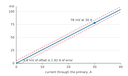
Two amps of error is invisible at 30 A and useless at 2 A, which is why Hall current sensors are specified by their full-scale range and are a poor choice for measuring small currents in a wide-range design. It is also why serious devices use chopper stabilisation, rotating the drive and sense contacts electrically at kilohertz rates so that the offset averages out while the true Hall signal does not. That technique is the single biggest reason modern Hall current sensors are usable at all, and it is also the reason they inject a small switching artefact into their own output.
Temperature is the other standing problem. Carrier density in a doped semiconductor changes with temperature, so both sensitivity and offset drift, and a datasheet's accuracy figure is nearly always dominated by temperature rather than by anything you can fix in the circuit. Ratiometric devices, whose output scales with their supply, cancel one term of this when the ADC shares the same reference — a useful trick that works only if you actually share the reference.
The alternatives are worth knowing. A shunt resistor is cheaper and more accurate but is galvanically connected to the circuit and dissipates power. A current transformer is isolated, accurate and lossless but cannot read DC, for the reason Layer 1 opened with. Magnetoresistive sensors beat Hall devices on sensitivity and drift and cost more. Hall wins where you need isolation, DC response and low cost together, which is a common enough corner to have made it ubiquitous.
Common mistakes
- Expecting a coil-based clamp meter to read DC — it cannot, at any price. A meter that reads DC current without breaking the circuit has a Hall element or a fluxgate in its jaws, and that is what the extra cost buys.
- Measuring the Hall voltage along the plate instead of across it — it appears at right angles to both the drive current and the field. Sensing contacts on the drive axis read the drive voltage and almost none of the signal.
- Using a metal as the sensing element — copper's Hall coefficient is millions of times too small. The effect is real in every conductor and useful in almost none of them.
- Ignoring offset at the bottom of the range — a fixed output offset becomes a fixed current error, so a sensor sized for 100 A will not tell you the difference between 1 A and 3 A.
- Assuming the field is perpendicular — only the component through the plate's face counts, and a tilt of sixty degrees halves the reading without any hint that something is wrong.
Frequently asked questions
What is the Hall effect?
It is the sideways voltage that appears across a current-carrying conductor when a magnetic field passes through it. The field deflects the moving carriers to one edge, and they accumulate there until their own electric field cancels the deflection.
Why do Hall sensors use semiconductors rather than metal?
Because the Hall voltage is inversely proportional to carrier density, and metals have far too many carriers. The same plate in copper produces nanovolts where doped silicon produces millivolts.
Can a Hall sensor measure DC current?
Yes, and that is its main advantage over a current transformer. It responds to the field itself rather than to changes in it, so it reads steady currents down to zero frequency.
What is the difference between a Hall switch, a latch and a linear device?
A switch turns on above a threshold field and off below it. A latch turns on with one magnetic polarity and stays on until it sees the other. A linear device outputs a voltage proportional to the field, which is what analogue measurement needs.
Why is the Hall voltage bigger in a thinner plate?
Because thickness appears in the denominator. The same current squeezed through a smaller cross-section means a higher carrier velocity, and a faster carrier is pushed harder sideways by the same field.
Does the Hall effect tell you anything besides the field strength?
Its sign tells you whether the charge carriers are electrons or holes, and combined with the material's conductivity it gives the carrier density. Both are routine semiconductor measurements rather than curiosities.