
Quick Answer
Pin numbering starts at a marked corner and runs anticlockwise as you look down at the top of the part. That order belongs to the chip and stays the same whatever package it is sold in. What changes with the package is board area, how hot the die runs, and which assembly tools can still reach the leads.
Intuition
The numbers are the part, not the box
House numbers on a street follow a rule, and the rule is the only reason a stranger can find number 47. Odds one side, evens the other, counting up from one end. Nobody has to be told: you find the low numbers, work out which way they climb, and walk.
The rule survives everything about the houses themselves. A terrace and a bungalow on the same street carry numbers from the same sequence. What changes between them is how much of the street each one takes up.
An integrated circuit's pins are numbered the same way, and for the same reason. There is a marked corner, there is a direction, and everything follows. The chip inside decides what each numbered pin does, and it decides that once, for every package that chip is ever sold in. The package decides something else entirely: how much board it eats, how hot the die gets, and whether you can solder it by hand.
Those two facts get muddled constantly, usually by someone who has just found the same part number in three different packages and wants to know which pinout to use. The answer is that there is one pinout. There are three sizes.
Practitioner
Finding pin 1, and going the right way round
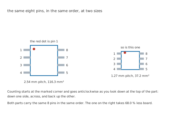
Both drawings are from above, which is how every datasheet draws a package and is not how the board sees it.
Manufacturers mark the pin-1 corner, and they do it in more than one way. A notch cut into one end of the body. A dot moulded or printed into one corner. A bevelled edge. Sometimes a chamfered corner on the die pad. On a board, a silkscreen dot, a squared-off pad, or a line down one side of the outline.
Once you have found it, the direction is fixed: anticlockwise, viewed from above.
Worked example — Counting round an eight-pin part
Pin 1 is at the marked corner. Going anticlockwise from there, the numbers run down that side to 4, cross the bottom, and come back up the far side.
On a part with 8 pins in two rows, that puts pin 5 diagonally opposite pin 4 and pin 8 directly opposite pin 1.
The same count on a four-sided package runs down one edge, along the bottom, up the far edge and back along the top. The rule is identical; there are simply more corners to turn.
That anticlockwise convention is the one thing here worth committing to memory, because everything else can be looked up and this is what tells you whether you are looking the wrong number up.
Two packages, one pinout
The two parts drawn above are the same eight signals. The smaller one runs at 1.27 mm pitch instead of 2.54 mm and covers 37.2 mm² of board instead of 116.3 mm² — 68.0 % less, for the same connections.
Nothing about pin 3 changed. Whatever pin 3 was on the large one, it is on the small one.
Engineer
What the package actually decides
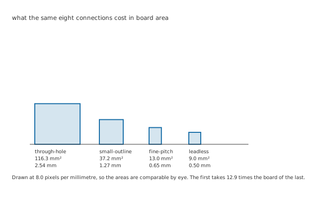
Drawn at eight pixels per millimetre, so the areas are comparable by eye rather than by caption.
Four invented packages carry the rest of this lesson: a through-hole part at 2.54 mm pitch, a small-outline part at 1.27 mm, a fine-pitch part at 0.65 mm, and a leadless part at 0.50 mm with a metal pad on its underside. Every number attached to them is an invention of this lesson and belongs to no catalogue part.
Board area falls faster than the pitch does
Worked example — Why halving the pitch does better than halving the area
The through-hole footprint is 11.4 mm by 10.2 mm, which is 116.3 mm².
The small-outline one is 6.0 mm by 6.2 mm, the fine-pitch one 3.1 mm by 4.2 mm for 13.0 mm², and the leadless one 3.0 mm by 3.0 mm, or 9.0 mm².
That is 12.9 times less board from a pitch only five times finer, because area falls with the square of the linear shrink.
The same arithmetic run the other way is why a coarse pitch runs out of edge so quickly. An edge 10 mm long takes 3.94 pins at 2.54 mm and 20.0 at 0.50 mm, which is 5.08 times as many. Past a certain pin count a coarse-pitch package stops being large and starts being impossible.
Smaller runs hotter, and then one of them does not
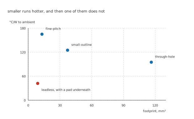
Three points on a trend and one that is not on it. The odd one is the one with a pad underneath.
A package's job includes getting heat out of the die and into the board, and a smaller package has less of everything to do it with.
Worked example — One die, four packages
The same die dissipates 400 mW in an ambient of 35 °C.
In the through-hole package at 95 °C/W the junction sits at 73.0 °C. The small-outline part at 125 °C/W reaches 85.0 °C, and the fine-pitch one at 165 °C/W reaches 101.0 °C.
The leadless part is the smallest of the four and the coolest: 42 °C/W puts it at 51.8 °C, which is 49.2 °C below the fine-pitch part.
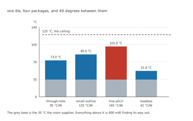
The grey base is the ambient the room supplies. Everything above it is 400 mW finding its way out.
The leadless part wins because it has a metal pad on its underside soldered flat to copper, so the heat leaves through the board rather than through eight thin legs. That is a construction difference, not a size one, and it is why a package family cannot be ranked on area alone.
Turned round, the same four numbers say what each package will let the die spend.
Worked example — How much dissipation each package allows
With a maximum junction temperature of 125 °C and the same 35 °C ambient, there is a fixed budget of ninety degrees to spend.
The through-hole part spends it at 947 mW, the fine-pitch part at 545 mW, and the leadless part at 2.14 W.
That last figure is 3.93 times the fine-pitch part's, from a package with a smaller footprint. A heatsink is the next step past all of them.
Professional
The two things that go wrong
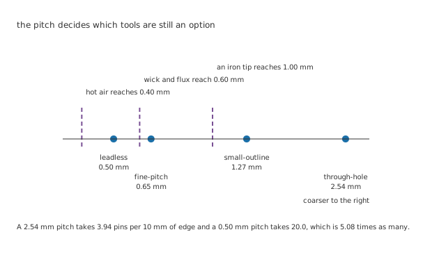
Every package sits to the right of exactly the thresholds it satisfies.
The pitch decides who can build it
A footprint is not only a size. It is a commitment about how the board gets assembled, and it is made at schematic time by someone who is usually thinking about something else.
Through-hole and small-outline pitches are reachable with an iron and a steady hand. Below about 0.60 mm an iron alone stops being enough and the technique changes: flood the pins with flux, drag the joint, and lift the excess with braid. The leadless part has no legs to reach at all — its pads are under the body, and it needs paste, a stencil and hot air, or a reflow oven.
None of that is a reason to avoid fine pitch. It is a reason to decide, before the board is laid out, who is going to build the first one. Joint quality is a separate skill and it does not rescue a footprint nobody in the building can assemble.
And the part goes in the wrong way round
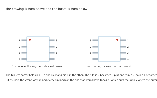
Two views of one part. The red pin-1 marker moves corners and every number moves with it.
Every datasheet drawing is from above. Every board is assembled by someone looking at it from above too, so the two agree and nobody thinks about it.
They stop agreeing the moment anything is viewed from underneath: a bottom-side placement, a footprint drawn mirrored, a socket adaptor, a part on the far side of a two-sided board being probed from the near side.
Worked example — What a mirrored footprint does
Mirror an 8 pin part and the pin at any physical position swaps with the pin facing it, so pin k becomes pin 8 plus one minus k.
Pin 8, the supply, lands where pin 1 was. Pin 4 lands where pin 5 was.
Nothing about that is subtle once it has happened. The supply now feeds an input, and the part is usually destroyed before anyone reads a voltage.
The check is quick and worth doing every time: find pin 1 on the silkscreen, find pin 1 in the datasheet drawing, and confirm they are the same corner of the same view. If the footprint came from a library rather than from the drawing, confirm it against the drawing anyway.
Reading a package designation
Package names carry information, and the information is not always what it looks like.
The letters name a family and a lead style. Through-hole, gull-wing surface mount, leadless, ball grid. They do not name a size on their own.
The number is usually the pin count, and occasionally the body width in tenths of an inch or in millimetres, which is why two packages with the same name and different numbers are sometimes the same size.
A suffix often names the thermal pad. The difference between 165 °C/W and 42 °C/W is exactly this kind of suffix, and it is the difference between 545 mW and 2.14 W of allowed dissipation.
And the drawing is the authority. A designation names a family; the dimensioned drawing in the datasheet names the part. Where a footprint library and a drawing disagree, the drawing is right and the library is somebody's assumption.
Common mistakes
- Assuming the pinout changed with the package — it does not. The same eight pins run in the same order on a 2.54 mm part and a 1.27 mm one; only 116.3 mm² becoming 37.2 mm² changed.
- Counting clockwise — the direction is anticlockwise from the marked corner, viewed from above. Counting the other way on an 8-pin part swaps pin 8 with pin 1 and pin 4 with pin 5, which is the same damage as fitting it upside down.
- Trusting a footprint library over the drawing — the library is a transcription of somebody's reading of the drawing. The dimensioned drawing is the part.
- Ranking packages on size for thermal purposes — the smallest of the four here is the coolest, at 42 °C/W against the fine-pitch part's 165 °C/W, because it has a pad underneath and the others do not.
- Choosing a fine pitch without asking who assembles it — 0.65 mm needs flux and braid rather than an iron alone, and a 0.50 mm leadless part needs paste and hot air. The decision is made at schematic time and paid for at build time.
- Reading a bottom-side part from the top-side drawing — a mirrored view maps pin k to pin 9 minus k on an 8-pin part, so probing what you think is the supply is probing an input.
Frequently asked questions
Which pin-1 marker do I trust when a part has two?
Both, and check they agree. A moulded dot and a notch on the same body should point at the same corner, and on almost every part they do. Where a printed marking disagrees with a moulded feature, the moulded one is the package and the printed one is ink, so the moulded feature wins. If they disagree and it matters, the dimensioned drawing settles it.
Does the anticlockwise rule hold for ball grid arrays too?
No, and that is the one common exception worth knowing. Ball grids are numbered as a grid rather than as a ring: letters down one axis and numbers across the other, with A1 at the marked corner. The idea is the same — a marked origin and a fixed direction — but the sequence is two-dimensional and reading it as a ring gives nonsense.
Can I put a surface-mount part on a through-hole footprint?
For a one-off, sometimes, with an adaptor board that carries the small footprint on one side and pins on the other. It is a legitimate repair and prototyping trick. What it does not do is fix the thermal problem: an adaptor puts the part further from copper, not closer, so a package that relied on its pad to reach 42 °C/W will not.
Why do datasheets give more than one thermal resistance?
Because one number cannot describe a path with several stages. A junction-to-case figure describes the die and the package alone; a junction-to-ambient figure includes the board, and therefore depends on how much copper the board has. The 95, 125, 165 and 42 °C/W here are all junction-to-ambient on one stated board, which is the only way they compare.
Is the largest package always the easiest to solder?
Nearly, but not quite. Lead pitch is what decides whether an iron can reach a joint, and a large package with many pins can have a finer pitch than a small one with few. The thing to look up is the pitch, not the body size, which is why the figure above puts pitch on its axis and nothing else.