
Quick Answer
An integrated circuit is a whole circuit built at once in a single piece of silicon: transistors, resistors and the wiring between them, made by the same sequence of steps. That gets you enormous component counts and parts that match each other closely, at the cost of area, heat, and anything that needs to be large.
Intuition
One plate, and then the copies are free
Before the printing press, a second copy of a book cost roughly what the first one had: a scribe, a desk, some months. After it, almost all the cost sat in cutting the plate, and the copies were paper and time. Two things changed at once. The price stopped tracking the number of copies, and every copy came out identical, because they all came off the same plate.
Silicon does both of those things to a circuit.
Building a transistor in a wafer takes a sequence of steps — grow an oxide, lay down a pattern, expose it, etch, dope, do it again — and that sequence costs the same whether the pattern being printed has one transistor in it or twelve thousand. So the price of a circuit stops tracking how many parts are in it and starts tracking how much room it takes up. And because every device on one piece of silicon was made in the same pass, by the same steps, on the same day, out of the same material, those devices resemble each other far more closely than two parts pulled from two different bins ever will.
That is the whole idea. Everything else in this lesson is what it costs you.
Practitioner
What one pass of the process actually makes
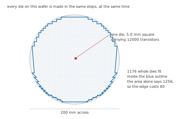
The grid is the die pattern, repeated. The blue staircase is where a whole one actually fits.
The starting material is a disc of silicon. This lesson works on an invented one: 200 mm across, which is 314 cm² of surface, ruled into square dies 5.0 mm on a side. Every die on it gets the same pattern, and the wafer goes through the process as one object. Every process figure in this lesson is invented the same way and belongs to no real foundry: the defect count, the matching, the oxide capacitance and the package's thermal resistance are all chosen to make the arithmetic legible, and a real foundry's are behind an agreement long before anyone shows them to you.
Worked example — How many chips come off one wafer
Each die takes 0.25 cm², so dividing the wafer's 314 cm² by that says 1256 of them fit.
Counting them properly says otherwise. A die has to sit entirely inside a circle, and the ones that hang over the edge are scrap, so the real count is 1176 — the area arithmetic overstates it by 80.
At 12000 transistors on each die, one trip through the process makes 14.1 million transistors, and every one of them was doped in the same step as all the others.
That last number is the part worth sitting with. Nobody placed those transistors. Nobody wired them. The pattern was drawn once, and the process printed it everywhere the wafer had room.
Every joint is another chance to be unlucky
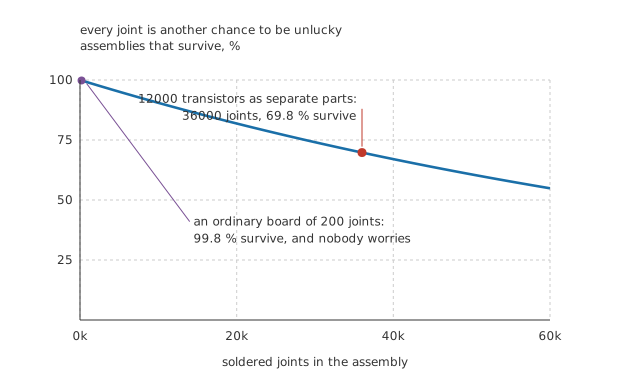
The curve never flattens. It just keeps taking its cut.
Cost is the argument people reach for first, and it is not the strongest one. The strongest one is that an integrated circuit has almost no connections in it.
A discrete bipolar transistor has three leads, and each of those leads becomes a soldered joint on a board. Joints are good — but they are not perfect, and the arithmetic of "not perfect" is unforgiving once you have a lot of them.
Worked example — The same circuit, built the hard way
Give every joint an independent chance of being bad of 0.0010 %. An ordinary board with 200 joints on it comes through intact 99.8 % of the time, which is why nobody thinks about this.
Now build 12000 transistors out of separate parts. At 3 leads each that is 36000 joints, and the same per-joint figure gives 69.8 % intact.
30.2 % of those assemblies have a fault in them somewhere before they are ever switched on.
On a die there is no solder anywhere. The connections are metal grown in place, in the same steps that made the devices, and they fail at rates that have nothing to do with the numbers above. That is why circuits got large: not because integration made them cheaper, but because it made them possible to finish.
Engineer
Matched, but not accurate
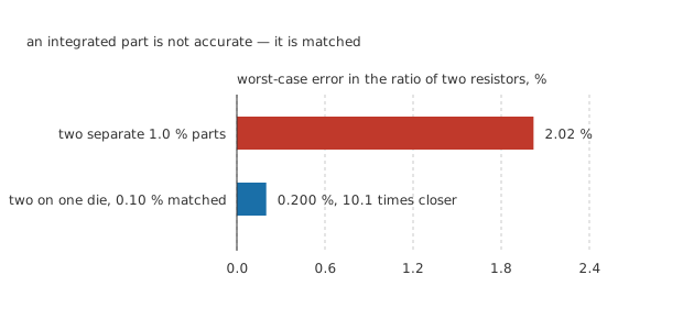
Both bars start at zero and neither has a pedestal, so the lengths are the numbers.
Here is where designers get caught. An integrated resistor is worse than a discrete one in absolute terms and much better in relative terms, and almost every analogue circuit on a chip is built to exploit exactly that.
The absolute value of an on-chip resistor depends on how thick a doped layer came out and how wide the pattern etched, and those wander across a wafer and between production runs. A spread of 20 % is normal and is not a defect. A discrete film resistor from a reel will beat that without trying.
But two on-chip resistors sitting a few micrometres apart went through every step together, so whatever wandered, wandered for both of them.
Worked example — What the ratio is worth, either way
Take two discrete parts, each specified to 1.0 %. Nothing stops one sitting at the top of its band and the other at the bottom, so their ratio can be out by 2.02 %.
Two made side by side on one die match each other to 0.10 %, so the same worst case gives 0.200 %.
That is 10.1 times closer, from parts whose absolute values you cannot trust at all.
This is the reason the next few lessons look the way they do. A gain set by a ratio of two resistors is accurate on a chip; a gain set by one resistor's absolute value is not. Chip designers write circuits in ratios wherever they possibly can, and where they cannot, they trim or they put the critical part outside.
The things that will not fit
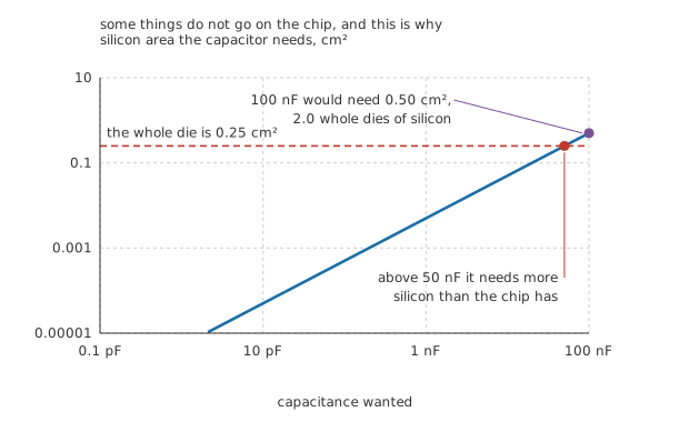
Both scales are logarithmic, and the die's own area is the horizontal rule.
Transistors shrink well. Capacitors do not, because capacitance is area divided by dielectric thickness, and once the dielectric is as thin as the process can make it the only lever left is area.
Worked example — Why the board still has capacitors on it
Take a declared oxide capacitance of 2.0 fF/µm². The die's own 0.25 cm² is then worth 50 nF and no more.
A 100 nF decoupling capacitor would need 0.50 cm² of silicon, which is 2.0 whole dies.
The chip would be a capacitor with a circuit as a rounding error.
Inductors are worse again, because a flat spiral of on-chip metal buys nanohenries, and anything that needs to store real energy needs volume that silicon does not have. Every switching supply on a board still has a wound inductor beside the chip, and it always will.
Professional
Area is the price, and heat is the ceiling
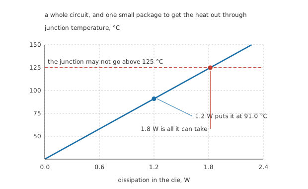
One straight line, starting at ambient, with a slope that is the package's thermal resistance.
A whole circuit in one small package means all of that circuit's heat leaves through one small package.
Worked example — What the package will take
The invented package here has 55 °C/W from junction to still air, in a 25 °C room, and its silicon may not go above 125 °C.
Dissipating 1.2 W puts the junction at 91.0 °C.
The limit is reached at 1.8 W, so the working point has a factor of 1.5 in hand — on a part with no metal on it anywhere.
Nothing about that number is generous, and it is why power devices stayed discrete long after everything else was integrated, and why a heatsink turns up the moment a chip is asked to do real work. A part that would be comfortable spread across four discrete transistors on a board can be at its limit in one package.
What each good die has to carry
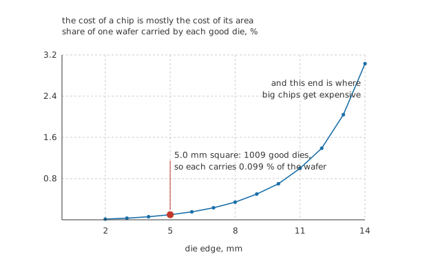
Thirteen die sizes, one wafer, and the same 180 defects scattered over all of them.
Since the process charges by the wafer, the sums come out per unit of area, and the yield makes them come out worse than that.
A wafer picks up flaws. A speck of dust during an exposure, a particle in an etch, a crystal defect in the substrate: each one lands somewhere, and a die it lands on is dead. Scatter them at random and the chance a given die escapes all of them follows the same shape as the joint arithmetic in layer two, for the same reason.
Worked example — From defects to what a chip costs
Put 180 killer defects at random on the wafer. Spread over 1176 dies that is 0.153 defects landing on the average die, so 85.8 % of them come out working.
That leaves 1009 saleable dies out of one wafer, and each has to carry 0.099 % of everything the wafer cost.
Double the die's edge and the area quadruples, so both terms move the wrong way at once: fewer dies to start with, and each of them likelier to catch something.
That is the shape in the last figure, and it is the single fact that governs what gets integrated. Big chips are not expensive because they are hard to design. They are expensive because area is the thing being sold, and yield charges compound interest on it.
Reading what you are handed
The word covers a range so wide it barely functions as a category. A jellybean op-amp has a few dozen transistors on a die a millimetre across; a processor has billions. Both are integrated circuits, and nothing else about them is comparable.
What is worth knowing about any of them, before the datasheet:
Analogue parts live or die by matching, so their datasheets talk about offsets, drift and how closely one thing tracks another, and hardly ever about the absolute value of anything inside.
Digital parts live or die by timing and by voltage thresholds, so their datasheets talk about propagation delays and the voltages that count as a one.
Every part has a supply range and a temperature range, and outside either of them the manufacturer has told you nothing about what happens.
The package is part of the specification, because the same die in a smaller package has a smaller ceiling, and that ceiling is what 55 °C/W was doing in the worked example above.
Common mistakes
- Trusting an on-chip resistor's value — the absolute spread is 20 % and that is the process working as designed. Use it in a ratio with another resistor on the same die, where the match is 0.10 %, or put the part that must be accurate outside the chip.
- Assuming integration always saves money — it saves money when the area is small. At 5.0 mm square each good die carries 0.099 % of a wafer; the same wafer yields only 33 dies at 14 mm square, and each of those carries 3.03 % of it.
- Sizing a chip's dissipation by its board area — a whole circuit in one package has one thermal path. 1.2 W through 55 °C/W is a junction at 91.0 °C, and the 125 °C limit arrives at 1.8 W.
- Expecting large passives to integrate — 100 nF would need 0.50 cm² of silicon, two whole dies, and inductors are worse. Decoupling capacitors and power inductors stay on the board.
- Reading "integrated" as "reliable" without knowing why — it is not the silicon that is unusually good, it is the absence of 36000 solder joints. Reliability arguments that ignore the interconnect are missing the actual mechanism.
- Treating the die count as wafer area divided by die area — that says 1256 for this wafer and the honest count is 1176. The 80 dies in between are the ones hanging over the edge, and on a large die that fraction grows fast.
Frequently asked questions
What actually makes an integrated circuit cheap?
Not the silicon, which is a small part of the cost, and not the transistors, which are effectively free once the pattern exists. It is that one sequence of process steps prints every device on the wafer at once, so cost tracks area rather than component count. A die twice as wide costs about four times as much before yield is even considered.
Why can chip designers not just use accurate resistors?
Because nothing about the process controls absolute values well. Layer thickness and etched width vary across a wafer and between runs, so a 20 % spread is ordinary. What the process does control is uniformity over short distances, so two resistors a few micrometres apart match to 0.10 % even though neither is close to its nominal value. Circuits are written in ratios to live inside that.
Why are there still discrete capacitors and inductors on every board?
Because both store energy in volume, and silicon has almost none to spare. At the oxide capacitance used here, the whole die is worth 50 nF; a single 100 nF decoupling capacitor would need 0.50 cm², or 2.0 whole dies. Inductors are worse still, since a flat spiral of on-chip metal gives nanohenries.
How does a defect on a wafer turn into a price?
Each killer defect kills whatever die it lands on. Spread 180 of them over 1176 dies and the average die sees 0.153 of a defect, which leaves 85.8 % of them working. The wafer's cost is then divided among 1009 good dies instead of 1176, and every step that makes the die larger makes both numbers worse at the same time.
Is a bigger package always better for heat?
It is usually better, but the useful question is the number rather than the size. A package is specified by its thermal resistance from junction to ambient, and that figure — 55 °C/W here — with the dissipation and the ambient is all you need. Everything else about the package is packaging.