
Quick Answer
A MOSFET controls a channel through a gate insulated from it by a thin oxide layer, so no steady current flows into the gate at all. Turned on, an enhancement device behaves as a resistance rather than a fixed voltage drop, and that resistance depends on how hard the gate is driven.
Intuition
Worked through the glass
Watch a shop-window display being worked from outside, through the glass, with magnets. Nothing passes through the pane. There is no hole, no shaft, no seal to fail. The field reaches through and the mechanism moves.
A MOSFET's gate does that to a piece of silicon. Between the gate and the channel sits a layer of oxide, which is glass, and the gate does not touch the silicon at any point. What it does is impose a field, and that field pulls charge carriers into a thin layer just under the oxide, turning what was insulating into a conducting channel.
The consequences of "no hole through the glass" are what the whole family is built on.
No steady gate current. A bipolar transistor needs base current the whole time it is on. A MOSFET needs a gate voltage, and once that voltage is established nothing more is taken. Driving one costs almost nothing while it sits still.
The on-state is a resistance, not a drop. A saturated bipolar transistor holds a few hundred millivolts across itself regardless of the current. A MOSFET turned on is a piece of conducting silicon, and the voltage across it is simply the current multiplied by its resistance — which at low current is a far better bargain.
The glass is thin, and it can be broken. Fifty nanometres of oxide is all that separates the gate from the channel, and putting too much voltage across it destroys the part instantly and permanently. That single weakness explains most of the handling rules the family comes with.
Practitioner
The structure, and what it is made of
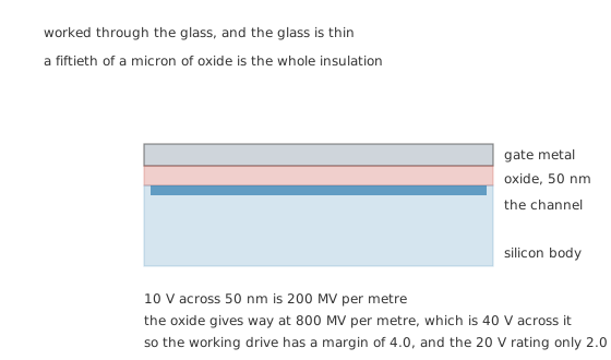
A fiftieth of a micron of oxide is the whole insulation.
Worked example — How close the gate runs to destruction
Silicon dioxide gives way at about 800 MV per metre. Across 50 nm of it, that is 40 V.
The working drive of 10 V puts 200 MV per metre across the layer, so it has a margin of 4.0.
The datasheet's maximum gate rating of 20 V leaves a margin of only 2.0. That is why the gate rating is an absolute maximum rather than a suggestion, and why a static discharge onto an unprotected gate is fatal rather than merely unwelcome.
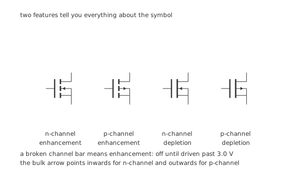
Two features tell you everything about the symbol.
The symbol carries exactly two pieces of information. A broken channel bar means enhancement — the device conducts nothing until the gate passes its threshold, and almost every power MOSFET in use is this type. A continuous bar means depletion, which conducts with no drive, like a JFET. The bulk arrow points towards the channel for n-channel and away for p-channel.
An n-channel enhancement device with a 3.0 V threshold is the part this lesson works through, and it is the one to assume unless told otherwise.
Engineer
On-resistance, and the two things that spoil it
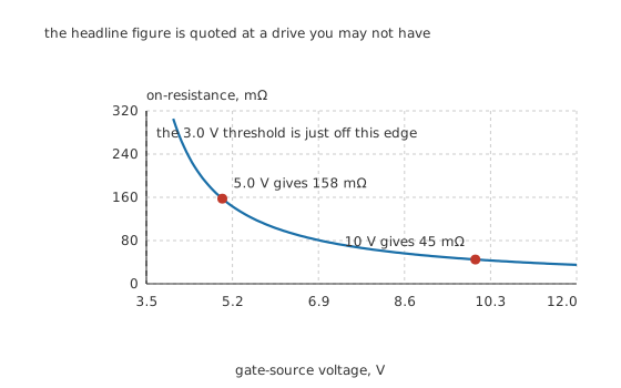
The headline figure is quoted at a drive you may not actually have.
Worked example — What a half-hearted gate drive costs
At the full 10 V drive this device is 45 mΩ.
Drive it from a 5.0 V logic rail instead and the same device becomes 158 mΩ — 3.5 times worse, and so 3.5 times the heat at the same current.
The curve rises steeply as the drive approaches the 3.0 V threshold, so the penalty grows quickly rather than gracefully.
A part whose on-resistance is quoted at 10 V and which is being driven from a 3.3 V logic pin may therefore be running at many times its headline figure.
That is the origin of "logic-level" MOSFETs, which are simply parts whose threshold has been made low enough that a logic rail is a full drive rather than a partial one. It is a selection matter rather than a circuit one: no amount of cleverness makes a standard part behave well on an inadequate gate voltage.
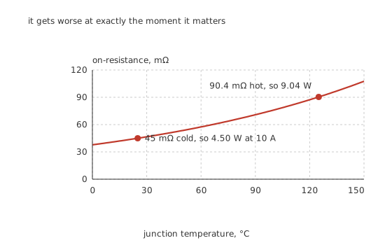
It gets worse at exactly the moment it matters.
Worked example — The factor of two nobody budgets for
On-resistance rises with temperature at about 0.0070 per degree. Between 25 °C and 125 °C that is a factor of 2.01, from 45 mΩ to 90.4 mΩ.
At 10 A the dissipation therefore goes from 4.50 W cold to 9.04 W hot.
A thermal design done at the datasheet's room-temperature figure is optimistic by a factor of two, and it is optimistic in a direction that feeds back on itself: more heat, more resistance, more heat.
The positive coefficient is not only a nuisance. It is what allows MOSFETs to be paralleled without individual ballasting — the device that takes more current gets hotter, its resistance rises, and it hands current back to its neighbours. A bipolar transistor's coefficient runs the other way, which is why thermal runaway is a bipolar problem rather than a MOSFET one.
Professional
The diode nobody fitted, and the limit nobody can design round
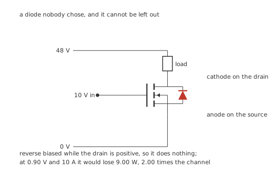
A diode nobody chose, and it cannot be left out.
Every power MOSFET contains a diode whether the designer wants it or not. The body region is tied internally to the source, and the junction between that body and the drain is a real diode with its anode at the source and its cathode at the drain.
Worked example — What that diode does, and what it costs when it conducts
With the drain positive — normal operation on a 48 V rail — the body diode is reverse biased and does nothing.
Pull the drain below the source, which is exactly what an inductive load does at turn-off, and it conducts at about 0.90 V. At 10 A that is 9.00 W.
Compare with the channel's own 4.50 W at the same current: the diode is 2.00 times worse. It will protect the device from an inductive kick, and it is a poor choice for anything that has to conduct for long.
A useful consequence and a dangerous one. Useful: a MOSFET switching an inductive load has its own freewheel path built in, and often needs no external flyback diode. Dangerous: a MOSFET cannot block current in both directions. Fitted backwards, or used to switch a battery whose polarity might reverse, it conducts through the body diode regardless of the gate, and the switch that is "off" is passing full current.
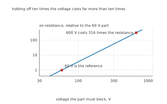
Ten times the voltage costs far more than ten times the loss.
Worked example — The silicon limit
Holding off more voltage needs a thicker, more lightly doped drift region, and that region is in series with the channel. Both the thickness and the doping work against you, so on-resistance grows roughly as the blocking voltage to the power of 2.5.
Take 60 V as the reference. A 600 V part of the same die area carries 316 times the on-resistance.
That relation is a property of silicon rather than of any manufacturer, which is why high-voltage switching reaches for an IGBT or for a wider-bandgap material instead of simply buying a better MOSFET.
Four handling and design rules the structure produces
Never leave a gate floating. With nothing connected, the gate holds whatever charge it acquires and the device can turn on unpredictably. A resistor from gate to source — ten to a hundred kilohms — costs nothing and defines the off state.
Protect the gate from static. The oxide's 40 V breakdown is reached by a discharge that a person cannot feel. Many parts include an internal zener across the gate; many do not, and the datasheet is the only way to know.
Treat the on-resistance figure as conditional. It is quoted at a stated gate voltage and a stated temperature, and both of those conditions move it by factors rather than percentages.
Check the body diode's rating and its recovery. In any bridge or synchronous arrangement the body diode conducts during the dead time, and its reverse recovery has to be swept out by the opposite device. That is a real loss and, in an H-bridge, a real failure mechanism.
Where the family goes next
How the channel forms is the physics under all of this. Using one as a switch is where the on-resistance figures earn their keep, and gate drive is where the "no gate current" claim gets its proper qualification — the gate takes no steady current, but it is a capacitor, and moving it costs charge every time.
Common mistakes
- Driving a standard MOSFET from a logic pin — at 5.0 V instead of 10 V this device is 158 mΩ rather than 45 mΩ, 3.5 times the heat. Use a logic-level part or a gate driver.
- Designing thermally at the room-temperature on-resistance — it doubles by 125 °C, from 45 mΩ to 90.4 mΩ, taking 4.50 W to 9.04 W at 10 A.
- Assuming a MOSFET blocks in both directions — the body diode conducts from source to drain whatever the gate does, so a reversed part or a reversed supply passes full current through an off switch.
- Leaving a gate floating — it holds whatever charge it collects and can turn the device on by itself. A gate-to-source resistor defines the off state.
- Treating the gate rating as advisory — 20 V against an oxide that breaks down at 40 V is a margin of 2.0, and exceeding it destroys the part permanently rather than tripping anything.
- Expecting a high-voltage part to behave like a low-voltage one — a 600 V device carries 316 times the on-resistance of a 60 V device of the same die area.
Frequently asked questions
Why does a MOSFET need no gate current when a bipolar transistor does?
Because the gate is separated from the channel by 50 nm of oxide, which is an insulator. The gate imposes a field rather than injecting carriers, so nothing flows through it in the steady state. It is still a capacitor, so charging and discharging it does cost current every time it switches.
What does on-resistance actually depend on?
The gate drive and the temperature, both strongly. At 10 V and 25 °C this part is 45 mΩ; at 5.0 V it is 158 mΩ, and at 125 °C it is 90.4 mΩ. The headline figure is quoted under stated conditions and moves by factors when those conditions change.
What is the body diode and can I get rid of it?
It is the junction between the device's internal body region, which is tied to the source, and the drain. It is part of the structure and cannot be removed. Its cathode is on the drain, so in normal operation with a positive drain it is reverse biased and idle; pulled the other way it conducts at about 0.90 V, which at 10 A is 9.00 W — twice what the channel loses.
Why does gate voltage destroy MOSFETs so easily?
Because the oxide breaks down at about 800 MV per metre, which across 50 nm is only 40 V. The 20 V gate rating is a margin of 2.0 against that, and once the oxide punctures the damage is permanent — there is nothing to reset.
Why are high-voltage MOSFETs so much worse than low-voltage ones?
Because the drift region that holds off the voltage is in series with the channel, and it has to be both thicker and more lightly doped as the rating rises. On-resistance grows roughly as the blocking voltage to the power of 2.5, so a 600 V part carries 316 times a 60 V part's resistance for the same die area.