
A stable bias holds its operating point despite the device's gain and its own heating. Both are achieved the same way: put resistance in the emitter path so the circuit, not the device, decides the current. Whether heating runs away depends on one loop gain, and it must be under one.
Intuition
Setting a current with something that will not stay still
Bias means choosing an operating point and then holding it. The difficulty is that a transistor changes, in two ways, and neither of them is under the designer's control.
Its current gain is not a specification, it is a range. Two devices from the same reel can differ by three to one, and the manufacturer does not promise otherwise. Any bias arrangement whose answer depends on the gain therefore has a three-to-one answer.
And its junction voltage falls as it warms. Around two millivolts per degree, which sounds negligible and is not, because the same device is turning current into heat as it works. Heat lowers the junction voltage; a lower junction voltage means more current; more current means more heat.
That is a loop, and loops have a property that the individual steps do not: they either settle or they do not. Round it once, and if what comes back is smaller than what went in, the disturbance dies out and the circuit finds a slightly warmer resting point. If what comes back is larger, nothing in the circuit stops it and the device destroys itself — thermal runaway, which is a real failure with a real criterion attached to it.
Both problems have the same cure and it is one component: resistance in the emitter path. A design that puts enough of it there is insensitive to gain and cannot run away. This lesson is about how much is enough, and what it costs.
Safety
Thermal runaway is a destructive failure, not a performance one: a stage whose loop gain exceeds one has no operating point to settle at, and it heats until something in it fails — occasionally loudly, in a package that is dissipating tens of watts. Every number in this lesson is an illustrative set chosen to make the arithmetic concrete, including the thermal resistance, the temperature coefficient and both current gains; none is taken from any standard or any real part, and a real design's margin must be worked out from its own figures.
Practitioner
The first problem: the device's gain
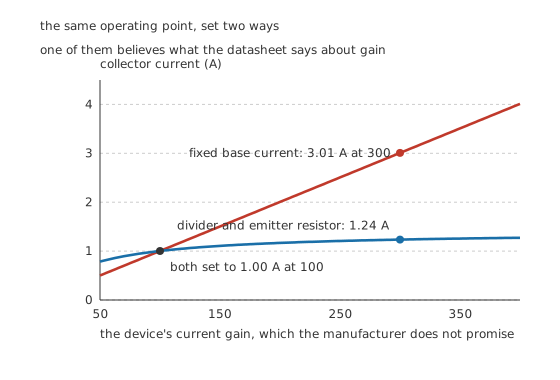
One of them believes what the datasheet says about gain.
Worked example — The same operating point, set two ways
Both arrangements are set to 1.00 A with a device whose gain is 100.
Fixed base current. A resistor of 1.87 kΩ from the 20 V rail delivers 10.0 mA into the base, and the collector current is whatever the gain makes of it. Hand the circuit a device of 300 and it draws 3.01 A — 200 % more.
A divider and an emitter resistor. A source of 1.40 V behind 20 Ω drives the base, and 0.50 Ω sits in the emitter. Now the current is set by the voltage left after the junction, divided by the emitter path, and the gain only enters through the small share of the source resistance the base current sees. The same three-to-one device gives 1.24 A — 23.2 % more.
8.61 times less sensitive, from one resistor.
The mechanism is negative feedback and nothing more exotic. More collector current means more emitter current, means more drop across the emitter resistor, means less voltage left across the junction, means less current. The circuit argues with itself and wins.
Engineer
The second problem: its own heat
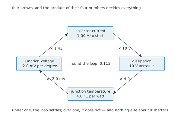
Four arrows, and the product of their four numbers decides everything.
The second problem is a loop, so it is worth drawing as one. Each arrow is a conversion with a number, and the numbers multiply.
Worked example — Round the loop once
The stage sits at 1.00 A with 10 V across the device, so it dissipates 10.0 W. In a package of 4.0 degrees per watt from an ambient of 25 °C, that puts the junction at 65.1 °C — a rise of 40.1 °C.
Now perturb it and follow the four arrows.
Current to power: each extra amp adds 10 V watts. Power to temperature: each extra watt adds 4.0 degrees. Temperature to junction voltage: each extra degree lowers it by -2.0 mV. Junction voltage to current: the emitter path is 698 mΩ — the resistor plus the source resistance referred through the gain — so each volt of extra drive produces 1.43 amps.
Multiply the four: 0.115.
Under one, so the loop settles. Any disturbance comes back smaller than it left, and the circuit finds a resting point slightly warmer than where it started.
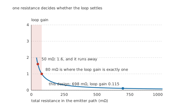
One resistance decides whether the loop settles.
Three of those four numbers are given to you: the device voltage by the circuit's job, the thermal resistance by the package, and the temperature coefficient by physics. Only the fourth is a design choice, and it appears in the denominator, which is why the loop gain is an inverse curve rather than a straight line.
Worked example — The criterion, in one line
Set the product to one and solve for the emitter path. The three fixed factors multiply to 80 mΩ — so any emitter path larger than that gives a loop gain under one, and any path smaller does not.
This design's 698 mΩ is nearly nine times that, so its loop gain is 0.115 and it is safe by a wide margin.
Cut the path to 50 mΩ — a small emitter resistor and a stiff drive, which is a perfectly ordinary thing to build — and the loop gain becomes 1.6. Above one, and there is no operating point for it to settle at.
Note what the criterion contains. A hotter package, a higher device voltage, or a bigger heatsink removed all push it the wrong way, and none of them is visible on the schematic.
Professional
Settling, running away, and what the cure costs
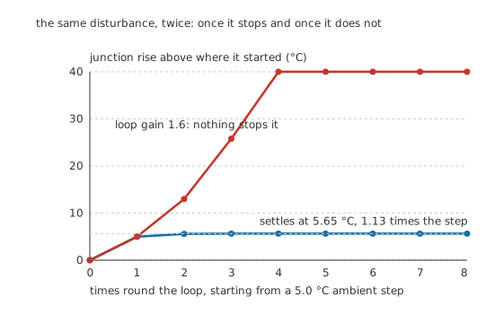
The same disturbance, twice: once it stops and once it does not.
Worked example — Following a five-degree disturbance
Give the circuit a 5.0 °C rise in ambient — a warm afternoon, or a lid put on the enclosure — and let it go round the loop.
With a loop gain of 0.115, each round adds a little over a tenth of the last: five degrees, then five and a half, then a fraction more, converging within a few rounds on 5.65 °C. That is 1.13 times the disturbance that caused it, and the collector current has risen by 16.2 mA.
With a loop gain of 1.6, each round is more than half again as large as the last. Five degrees, thirteen, twenty-six, and the trace leaves the top of the figure before eight rounds are done. Nothing in the arithmetic stops it, and nothing in the circuit stops it either.
The two traces come from the same equation with one number changed. That is what makes runaway hard to spot on a bench: a stage with a loop gain of 0.9 works, warms up, and works, and a nominally identical one at 1.1 does not survive being switched on twice.
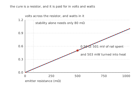
The cure is a resistor, and it is paid for in volts and watts.
Worked example — What the resistor takes
At 1.00 A through 0.50 Ω, the emitter resistor takes 501 mV of the rail and turns 503 mW into heat.
Half a volt out of 20 V is a little over two per cent of the supply, and half a watt out of 10.0 W is a similar share. Both are ordinary prices.
And notice how much of it thermal safety actually needed. The criterion asked for 80 mΩ; the design has 698 mΩ. The extra was bought for the gain insensitivity of the second layer, not for the runaway margin of the third — the same component solving two problems, sized by the harder of them.
Four things that follow
The loop gain is worst where the device is working hardest. It contains the device's voltage, so a stage that passes through a high-voltage, high-current state — a linear regulator dropping a lot, a class-AB stage at moderate output — has a higher loop gain there than at either extreme. Check the criterion at the worst point, not at the nominal one.
Better cooling makes the loop safer, and better coupling to the bias makes it safer still. Halving the thermal resistance halves the loop gain. Mounting the bias reference on the same heatsink removes the temperature term almost entirely, which is the arrangement a push-pull output stage depends on.
MOSFETs mostly do not have this problem, and sometimes do. A MOSFET's on-resistance rises with temperature, which is negative feedback rather than positive, so a switching MOSFET is inherently stable and can be paralleled. But a MOSFET in its linear region, biased near threshold, has a temperature coefficient that goes the other way — and the same loop criterion applies to it.
Emitter resistors are what make devices shareable. Two transistors in parallel are two loops sharing one heat path, and without individual emitter resistors the hotter one takes the current, gets hotter, and takes more. It is the same criterion applied between two devices instead of between a device and itself.
Common mistakes
- Biasing with a single base resistor — the collector current is then the base current times a gain the manufacturer does not promise, and a three-to-one device spread gives 1.00 A or 3.01 A.
- Checking the loop gain only at the nominal operating point — it contains the device voltage, so it is highest where the device is dropping the most, which is usually not the nominal point.
- Assuming a small emitter resistor is enough — the criterion here is 80 mΩ of total emitter path, and a design at 50 mΩ has a loop gain of 1.6 and no resting point at all.
- Forgetting the source resistance in the emitter path — the base's driving resistance divided by the gain plus one is part of it, and here it is 198 mΩ of the 698 mΩ total.
- Treating a working prototype as proof — a loop gain just under one works and one just over it does not, and the difference is invisible on a schematic.
- Paralleling devices without individual emitter resistors — that is the same loop running between two devices, and it settles on one of them taking everything.
Frequently asked questions
Why is a divider bias so much better than a single base resistor?
Because the current is then set by the circuit rather than by the device. A fixed base current gives 1.00 A at a gain of 100 and 3.01 A at 300 — 200 % more. The same three-to-one spread with a divider and an emitter resistor moves the current only 23.2 %, which is 8.61 times less sensitive.
What exactly is thermal runaway?
A feedback loop with a gain above one. Current makes power, power makes junction temperature, temperature lowers the junction voltage, and a lower junction voltage makes more current. Multiply the four conversions: 10 V per amp, 4.0 degrees per watt, -2.0 mV per degree and 1.43 amps per volt give 0.115 here — safely under one.
How much emitter resistance do I need?
Enough that the loop gain is under one, with margin. The three fixed factors multiply to 80 mΩ, so any emitter path larger than that is stable in principle. This design's 698 mΩ gives a loop gain of 0.115, and most of that resistance was bought for gain insensitivity rather than for the thermal margin.
What does a stable loop actually do when the circuit warms up?
It settles slightly warmer. A 5.0 °C rise in ambient converges within a few rounds on 5.65 °C at the junction — 1.13 times the disturbance — and the collector current rises by 16.2 mA. The loop amplifies the disturbance by a bounded factor rather than eliminating it.
What does the emitter resistor cost?
At 1.00 A through 0.50 Ω, 501 mV of the 20 V rail and 503 mW of heat — roughly two and a half per cent of the supply and five per cent of the device's own 10.0 W. That is the normal price, and it buys both the gain insensitivity and the thermal margin at once.
Knowledge check
Compare a fixed base resistor with a divider-and-emitter bias across a three-to-one gain spread. (Show answer)
Work out the thermal loop gain for this stage. (Show answer)
What emitter path does stability require, and what happens below it? (Show answer)
A 5.0 °C rise in ambient reaches a stable stage. Where does it end up? (Show answer)
What does the emitter resistor cost at this operating point? (Show answer)
One email a month from the bench
New circuits, lessons, part guides and calculators, on the first Sunday of each month.