
A push-pull output stage uses an NPN device to source current into the load and a PNP to sink it, each idle for half the waveform. Left unbiased it produces a dead zone at every zero crossing; a small forward bias between the two bases removes it, at the cost of a standing current.
Intuition
One pushes, the other pulls
A single transistor driving a load has an awkward problem: it can only pull in one direction. To make an output that swings both ways it has to sit at half the supply and idle there, pouring current through itself the whole time it is doing nothing. That works and it is called class A, and it wastes most of what it draws.
A push-pull stage splits the job in two. One device, connected to the positive rail, handles everything above zero — it sources current into the load. A complementary device, connected to the negative rail, handles everything below — it sinks current out of it. Each one is asleep for half the waveform, and neither has to idle at half the supply.
That halves the devices' working time and removes the standing current, which is why every audio amplifier, every motor driver and every op-amp output stage is built this way.
But there is a seam where the two halves meet, and it is right at zero — where quiet signals live. A transistor does not begin conducting until its junction is forward-biased by something like seven-tenths of a volt, so around zero there is a band in which neither device has woken up and the output does nothing at all.
Handing the signal from one device to the other cleanly, across that seam, is what the rest of this lesson is about.
Safety
An output stage of this kind turns real power into heat in two small packages, and the heatsinks it needs stay hot long after the supply is switched off. The quiescent bias described here is also, if it goes wrong, a mechanism for destroying the stage: with a bias that fails to track the devices' temperature, the standing current climbs as they warm and the warming climbs with it. Every number in this lesson — supply, load, junction drop, emitter resistance and temperature coefficient — is an illustrative set chosen to make the arithmetic concrete, and none is taken from any standard or any real part.
Practitioner
The circuit, and the seam in the middle
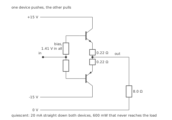
One device pushes, the other pulls.
Three things on that schematic are worth finding before anything else.
Both collectors face their own rail and both emitters face the output. That makes each device an emitter follower — unity voltage gain, large current gain — and it is what allows the pair to follow the input rather than invert it. Drawn the other way up, with the collectors at the output, the stage would be a complementary common-emitter pair, which inverts and behaves very differently.
The load returns to ground, not to a rail. The split supply is what lets the output swing symmetrically either side of zero without a coupling capacitor.
There are two small resistors in the emitters, and they look like a mistake in a stage whose whole point is efficiency. They earn their place in the fourth layer.
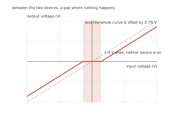
Between the two devices, a gap where nothing happens.
Worked example — How wide the seam is
The NPN needs its base 0.70 V above the output before it conducts. The PNP needs its base 0.70 V below.
With the two bases tied together — no bias at all — there is a band of input, 1.4 V wide, in which neither condition is met and the output stays exactly at zero.
Outside the band the output does follow the input, at unity slope, but shifted by 0.70 V: it never catches up with where it should have been.
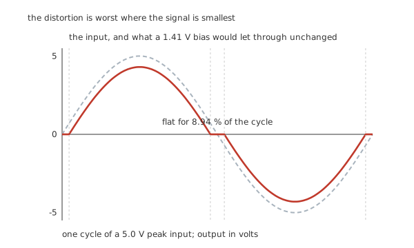
The distortion is worst where the signal is smallest.
Worked example — What the seam does to a waveform
Put a 5.0 V peak sine in. The output is flat at zero while the input is inside the dead band — twice per cycle, once at each zero crossing.
Working out how much of the cycle that is: the input's magnitude is below 0.70 V for the phases whose sine is smaller than the ratio of the two, which comes to 8.94 % of the cycle.
And that fraction gets worse as the signal gets smaller. A large signal spends a small proportion of its time crossing the band; a quiet one spends most of its time inside it. This is crossover distortion, and it is unusual in being a distortion that grows as the signal shrinks — which is exactly the opposite of how clipping behaves, and much more objectionable to listen to.
Engineer
Closing the seam, and what the stage delivers
The cure is straightforward to state: hold the two bases apart by just enough voltage to keep both devices on the edge of conducting. Then neither has to wake up; both are already awake, and the handover between them is continuous.
Worked example — The bias, and the standing current it buys
Both junctions need 0.70 V each, so the bias must supply 1.4 V — plus whatever the standing current drops across the two emitter resistors.
At 20 mA through 0.22 Ω in each emitter, that is 8.8 mV more: 1.41 V in total.
The price is that 20 mA flows straight down through both devices from one rail to the other, without ever reaching the load: 600 mW burned at idle.
This is class AB — not class A, because the standing current is a small fraction of the load current rather than all of it; not class B, because it is not zero. The choice of how much bias is the choice of where on that line to sit.
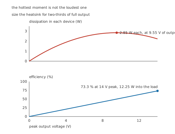
The hottest moment is not the loudest one.
Worked example — What it delivers, and what it costs to deliver
At full output. Each device needs some voltage across it to work, so the peak swing is 1.0 V short of the rail: 14 V. Into 8.0 Ω that sine delivers 12.25 W.
Drawing it costs 16.7 W from the 15 V rails, so the efficiency is 73.3 % — against roughly a third of that for a class A stage doing the same job.
And efficiency is in direct proportion to output. Half the swing, half the efficiency. A stage playing quietly is not an efficient stage; it is a stage wasting almost everything it draws.
The heat does not follow the output. Each device's dissipation is the difference between what the supply gives and what the load takes, and that difference peaks in the middle: 2.85 W per device at an output of 9.55 V, and less than that at full output.
So the heatsink is not sized for full power. It is sized for about two-thirds of full swing, which is where the stage is at its most uncomfortable.
Professional
The bias has to move
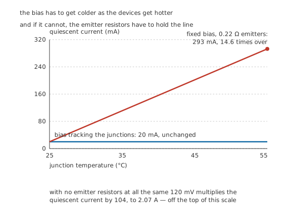
The bias has to get colder as the devices get hotter.
The bias worked out above is correct at one temperature and wrong at every other one, because a junction's forward voltage falls as it warms. Give the devices a fixed 1.41 V and, as they heat up, that becomes more bias than they need.
Worked example — What a thirty-degree rise does
Each junction's turn-on falls at -2.0 mV per degree. Over 30 °C from 25 °C, that takes it from 0.70 V to 640 mV.
Two junctions, so the fixed bias is now 120 mV more than the pair asks for. That surplus appears across the two emitter resistors and drives 273 mA of extra standing current: 293 mA, which is 14.6 times what it was set to.
And now take the emitter resistors away. The same 120 mV is then applied directly to two exponential junctions, and at 25.9 mV it multiplies the current by 104 — to 2.07 A, which no small-signal bias arrangement survives.
That is what the two small resistors are for. They convert an exponential dependence into a linear one, and they turn destruction into a specification.
The complete answer needs both halves. The emitter resistors bound the sensitivity; a bias that tracks the devices' temperature removes it. In practice that means the bias element is itself a junction — a pair of diodes, or a transistor wired as an adjustable multiple of its own base-emitter voltage — mounted on the same heatsink as the output devices, so that when they get hot it gets hot and gives back exactly the voltage they no longer need. The blue line on the figure is what that arrangement buys.
Four things that follow
The bias element is a thermal component, not an electrical one. It has to be on the heatsink. Left on the circuit board it tracks the ambient temperature rather than the junctions, and the stage behaves as the fixed-bias line does — slowly, over minutes, which is what makes it hard to diagnose.
Emitter resistors cost output and gain a little. They drop voltage that could have gone to the load, and they add local feedback that lowers the stage's output impedance. Typical values are a fraction of an ohm — large enough to bound the current, small enough not to matter into a load twenty times bigger.
A Darlington or Sziklai arrangement usually replaces the single devices. An output stage carrying amps needs base current the driver cannot supply, so each half becomes a composite. The bias then has to cover four junctions rather than two, and everything in this layer applies with the number doubled.
Crossover distortion is why class B is rare and class AB is everywhere. Zero bias gives the best efficiency and the worst distortion where the ear is most sensitive. A few tens of milliamps of standing current costs well under a watt and removes the effect entirely, which is a trade almost every design makes.
Common mistakes
- Leaving the stage unbiased to save power — 600 mW of standing current buys the removal of a distortion that occupies 8.94 % of the cycle at a 5.0 V input and a far larger share at small ones.
- Mounting the bias element on the board instead of the heatsink — it then tracks ambient rather than junction temperature, and the standing current drifts to 293 mA over a 30 °C rise.
- Omitting the emitter resistors — without them the same 120 mV of surplus bias multiplies the standing current by 104, to 2.07 A.
- Sizing the heatsink for full output — each device peaks at 2.85 W when the output is 9.55 V, not at the 14 V peak where the stage delivers its full 12.25 W.
- Drawing the pair with the collectors at the output — that is a complementary common-emitter arrangement, which inverts. In a push-pull follower both emitters face the output and both collectors face their own rail.
- Expecting the quoted efficiency at any volume — 73.3 % is the figure at full swing only; efficiency is in direct proportion to output, so a quiet stage is an inefficient one.
Frequently asked questions
What exactly is crossover distortion?
The flat spot an unbiased complementary pair produces at every zero crossing. Neither device conducts until its junction is forward-biased by 0.70 V, so there is a 1.4 V band of input that produces no output at all — 8.94 % of the cycle for a 5.0 V peak sine, and a far greater share for a smaller one.
How much bias does the stage need?
Enough to hold both junctions on the edge of conducting: 1.4 V for the two junctions, plus 8.8 mV across the emitter resistors at the chosen standing current — 1.41 V in total, which buys 20 mA of quiescent current and costs 600 mW at idle.
Why must the bias track temperature?
Because a junction's forward voltage falls by about 2.0 mV per degree. Over a 30 °C rise the two junctions need 120 mV less than a fixed bias is giving them, and that surplus pushes the standing current from 20 mA to 293 mA — 14.6 times over, and rising as the extra current heats the devices further.
What are the emitter resistors for?
They convert an exponential problem into a linear one. Without them, 120 mV of surplus bias multiplies the standing current by 104, to 2.07 A. With 0.22 Ω in each emitter the same surplus adds only 273 mA, which is survivable and predictable.
Where should the heatsink be sized?
For about two-thirds of full swing. Each device's dissipation peaks at 2.85 W when the output is 9.55 V and falls again by full output — so a stage sized for its 12.25 W maximum output would be under-cooled at the level it is most likely to sit at.
Knowledge check
How wide is the dead zone in an unbiased complementary pair, and what does it do to a 5.0 V peak sine? (Show answer)
What bias closes it, and what does the bias cost? (Show answer)
What does the stage deliver at full output, and at what efficiency? (Show answer)
Where is each device hottest? (Show answer)
What happens to the standing current if the bias does not track a 30 °C rise? (Show answer)
One email a month from the bench
New circuits, lessons, part guides and calculators, on the first Sunday of each month.