
A Darlington pair feeds one transistor's emitter into a second transistor's base, with both collectors joined. The composite behaves as one device whose current gain is roughly the product of the two, needing two junction drops at its input and holding a much higher saturation voltage at its output.
Intuition
A lever on the end of a lever
One lever multiplies a force by the ratio of its arms. Put the output of one lever onto the input of a second and the ratios multiply, so two modest levers give an enormous mechanical advantage between them. Nothing new has been invented; the same two parts have simply been arranged in series.
A Darlington pair does that with current gain. The first transistor's emitter current becomes the second transistor's base current, and since each multiplies what it is given, the pair multiplies twice.
The consequence is dramatic and the costs are equally so, which is why the arrangement is worth understanding rather than reaching for.
What you get: a device that needs microamps at its input to control amps at its output. Any logic pin can drive it directly.
What you pay, first: the input now has two junctions in series, so it needs about twice the voltage to turn on. That is a nuisance rather than a problem.
What you pay, and this is the real cost: the pair cannot saturate properly. The second transistor's base is held one junction drop above its emitter, and the first transistor's own saturation voltage sits on top of that, so the composite's collector can never come closer to its emitter than about nine hundred millivolts. At any serious current that is a lot of heat.
And what you have to remember: the second transistor's base has no discharge path except through the first, which is off when you want the pair off. Without a resistor across that junction the pair turns off slowly and drifts on by itself as it warms.
Practitioner
The arrangement, and the resistor that has to be there
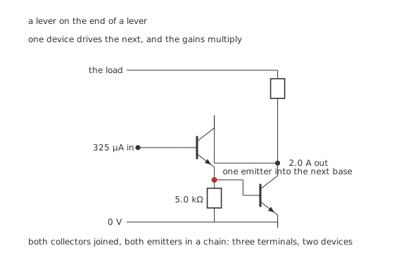
One device drives the next, and the gains multiply.
Worked example — The composite gain
Two ordinary devices of gain 100 and 60 give a composite of 6160.
That is their product plus each of them separately, because the first device's own collector current joins the second's at the shared collector node rather than disappearing.
At the product's size the two extra terms are barely worth the ink, but the expression is the exact one and the terms are real.
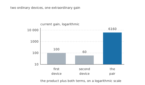
Two ordinary devices, one extraordinary gain.
Worked example — What that gain is worth at the input
Switching 2.0 A through the pair takes 325 µA of base current.
The second device alone, at its gain of 60, would have taken 33.3 mA — 103 times more.
That is not a marginal improvement. It is the difference between a load a microcontroller pin can switch and one it cannot.
Engineer
What it costs at both ends
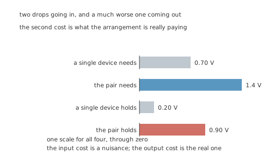
The second cost is what the arrangement is really paying.
Worked example — The two costs, separated
At the input, the pair needs 1.4 V against a single device's 0.70 V, because two junctions are in series. On a five-volt logic rail that is a modest fraction; on a rail under two volts it may be most of what is available.
At the output, the pair holds 0.90 V against a single device's 0.20 V. The mechanism is worth stating precisely: the second device's base has to sit a junction drop above its own emitter for it to conduct at all, and the first device's collector — which is tied to the composite's collector — can only get down to its own saturation voltage below that base. So the composite's floor is one junction drop plus one saturation voltage, and no amount of drive changes it.
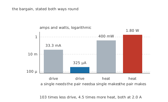
The bargain, stated both ways round.
Worked example — The trade, in numbers
At 2.0 A, the pair dissipates 1.80 W against a single device's 400 mW — 4.5 times more.
Meanwhile the drive it needs costs 455 µW, against the single device's 23.3 mW.
The drive saving is real but it is measured in milliwatts, and the heat penalty is measured in watts. A Darlington is not chosen to save power; it is chosen because the drive is not available at any power.
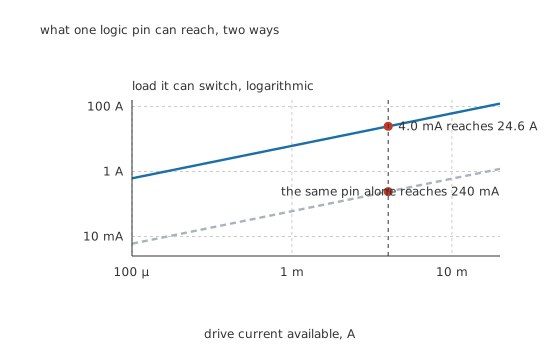
What one logic pin can reach, two ways.
Worked example — The argument that actually decides it
A logic pin able to source 4.0 mA can switch 240 mA through a single device.
Through the pair, the same pin reaches 24.6 A.
Below a certain drive capability the single device simply cannot do the job — not inefficiently, not at all — and that, rather than any efficiency argument, is when the pair earns its saturation voltage.
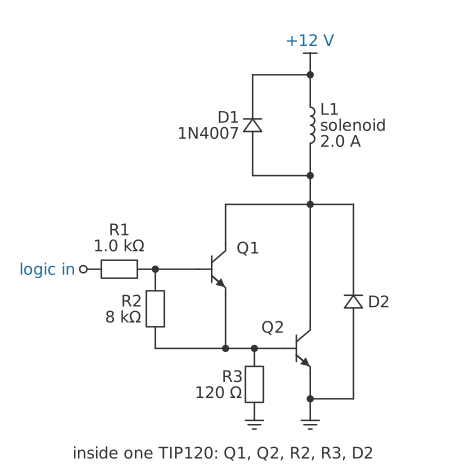
A real part puts the pair and its resistors in one package. A TIP120 driven from a 5.0 V pin through 1.0 kΩ takes 3.6 mA of base current, within what one pin can give, and switches 2.0 A. Its two bleed resistors, 8 kΩ and 120 Ω, are already inside, along with a diode from emitter to collector.
Professional
The resistor, and when to reach for something else
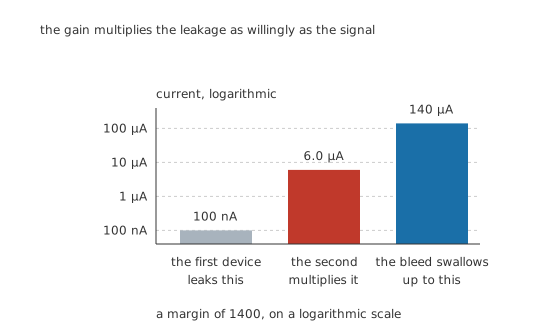
The gain multiplies the leakage as willingly as the signal.
Worked example — Why the bleed resistor is not optional
The first device's leakage of 100 nA arrives at the second device's base and is multiplied to 6.0 µA at the output. Leakage roughly doubles every ten degrees, so a warm pair can drift on by itself.
Fit 5.0 kΩ across the second device's base-emitter junction. That leakage now develops only 500 µV across it, nowhere near turning the junction on, and the resistor would swallow up to 140 µA before the junction began to conduct — a margin of 1400.
The same resistor does the second job too. When the drive goes away, the second device's base charge has no path out except through the first device, which is now off. The bleed gives it one, and without it the pair turns off far more slowly than either device would alone.
Integrated Darlington packages contain this resistor already, along with a second across the first device's junction and often a flyback diode. That is a large part of why a packaged Darlington is usually the better buy than two discrete transistors wired as one.
Four consequences to design around
It is a slow device. Two junctions in series, no discharge path except the bleed, and stored charge in both — a Darlington's turn-off is markedly worse than either transistor's. At switching frequencies it is the wrong answer, and a MOSFET is the right one.
Its saturation voltage sets the heatsink. 1.80 W at 2.0 A is not a small dissipation, and the thermal chain has to carry it. Doubling the load current doubles that figure, since the saturation voltage barely moves.
It multiplies gain variation too. Each device's gain varies by a factor of three, so the composite can vary by nine. That is fine for a switch designed to a forced gain and useless for anything that needs a defined gain.
The two devices need not be alike. A small signal device driving a large power device is the usual arrangement, because the first only ever carries a fraction of the load current. Their gains are then very different, and the composite is dominated by the product regardless.
Where the arrangement goes instead
The Sziklai pair solves the input-voltage problem by using complementary devices, so the composite needs only one junction drop at its input and saturates to one junction drop rather than a junction plus a saturation voltage. It is the standard alternative wherever the Darlington's drops are the objection, and it appears in almost every push-pull output stage for exactly that reason.
A MOSFET solves the drive problem completely rather than by multiplication: its gate takes no steady current at all, and its on-state is a resistance rather than a fixed drop, so at moderate currents it dissipates far less than either arrangement. Where the supply can provide a proper gate voltage, that is usually the modern answer.
Common mistakes
- Expecting it to saturate like a single transistor — the pair holds 0.90 V against a single device's 0.20 V, which at 2.0 A is 1.80 W rather than 400 mW.
- Leaving out the bleed resistor — the second device's base has no discharge path except through the first, which is off, and the first device's 100 nA of leakage is multiplied to 6.0 µA at the output.
- Driving it from a 1.8 V rail — the input needs 1.4 V for two junctions, which leaves almost nothing for the base resistor to work with.
- Choosing it to save power — the drive saving is 23.3 mW against 455 µW, and the heat penalty is 1.40 W. It is chosen when the drive is not available, not when it is expensive.
- Using it above audio switching speeds — two junctions, stored charge in both and only a bleed resistor to remove it make turn-off far worse than either device alone.
- Expecting a defined gain — each device's gain varies threefold, so the composite can vary ninefold.
Frequently asked questions
How much gain does a Darlington pair actually have?
The product of the two gains plus each of them: devices of 100 and 60 give 6160. The extra terms come from the first device's own collector current joining the second's at the shared collector node, and at that size they barely matter — but the expression is exact.
Why can't a Darlington saturate properly?
Because the second device's base must sit a junction drop above its own emitter to conduct, and the first device's collector — which is the composite's collector — can only get down to its own saturation voltage below that base. The floor is therefore a junction drop plus a saturation voltage, about 0.90 V here, whatever the drive.
What is the bleed resistor for?
Two things. It swallows the first device's leakage, which the second would otherwise multiply — 100 nA becoming 6.0 µA at the output — and it gives the second device's base a discharge path at turn-off, which it has nowhere else because the first device is off by then. 5.0 kΩ here gives a margin of 1400 against the leakage.
When is a Darlington the right choice?
When the available drive current is the constraint. A 4.0 mA logic pin reaches 240 mA through a single device of gain 60 and 24.6 A through the pair. Below a certain drive capability the single device cannot do the job at all, and that is the case the arrangement exists for.
What should I use instead?
A Sziklai pair where the junction drops are the objection — it needs one drop in and saturates to one drop out. A MOSFET where the supply can provide a proper gate voltage, since its gate takes no steady current and its on-state is a resistance rather than a fixed drop.
Knowledge check
Two transistors of gain 100 and 60 are wired as a Darlington. What is the composite gain and what drive does 2.0 A need? (Show answer)
What does the pair cost at its input and at its output? (Show answer)
Compare what the two arrangements dissipate at 2.0 A. (Show answer)
Why is the bleed resistor across the second device's junction necessary? (Show answer)
What load can a 4.0 mA logic pin switch each way? (Show answer)
One email a month from the bench
New circuits, lessons, part guides and calculators, on the first Sunday of each month.