
Used as a switch, a transistor is driven hard into saturation rather than operated on its gain. The base resistor is chosen so that even the lowest-gain device gets several times the base current it needs, which guarantees a low on-state voltage at the cost of a slower turn-off.
Intuition
Turning the handle past the stop
A tap that is fully open does not care how much further the handle would have gone. Turning it another half turn changes nothing about the flow and costs nothing but effort. What it does buy is certainty: whatever the tap, whoever fitted it, however stiff the washer, a handle turned past the stop is definitely open.
A transistor used as a switch is driven the same way. It is given several times the base current it needs, not because the extra does anything useful, but because the gain varies enormously and the extra guarantees that the worst device on the reel still saturates.
That changes the design question completely. An amplifier asks what the gain is; a switch asks what the gain is at least. The first is unanswerable and the second is on the datasheet.
Saturated, the device holds a couple of hundred millivolts across itself whatever the current, so it dissipates very little and the load gets almost all the supply. That is the point of the arrangement: the same package that would burn up holding a load halfway can switch it all day.
The one thing the extra drive costs is time. Overdriving the base fills it with charge that has to be removed before the device can turn off again, so the collector sits still for a while after the drive has gone. For a relay that does not matter at all. For anything switching fast it is the limit.
Practitioner
Designing the base resistor
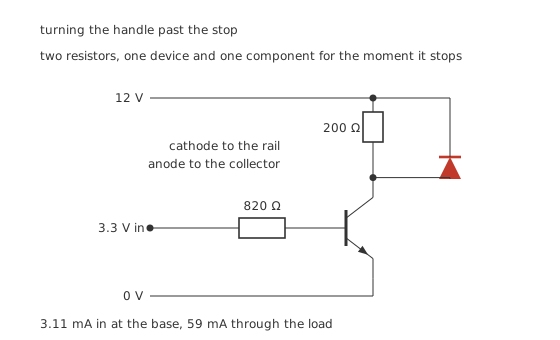
Two resistors, one device, and one component for the moment it stops.
Worked example — The whole design, in four steps
Find the load current. A 200 Ω load on 12 V, with 0.20 V lost in the device, takes 59 mA.
Find the base current the worst device needs. At a guaranteed minimum gain of 40, that is 1.48 mA.
Supply several times it. From a 3.3 V pin, with 0.75 V across the junction, 820 Ω passes 3.11 mA.
Check the margin. The forced gain is 19.0, well under the device's 40, giving an overdrive of 2.11.
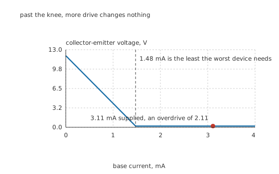
Past the knee, more drive changes nothing.
That curve is why the design works. Below the knee the collector sits partway up the rail and the device is dissipating heavily; above it the collector is on the floor and stays there. The whole art is to be comfortably to the right of a knee whose position you do not know exactly, and overdrive is how that is bought.
The flyback diode is not optional for an inductive load. Its cathode goes to the rail and its anode to the collector, so it does nothing in either steady state and conducts only in the instant after turn-off. Fitted the other way up it shorts the supply through the load the moment power is applied.
Engineer
What the overdrive costs, and where the drive comes from
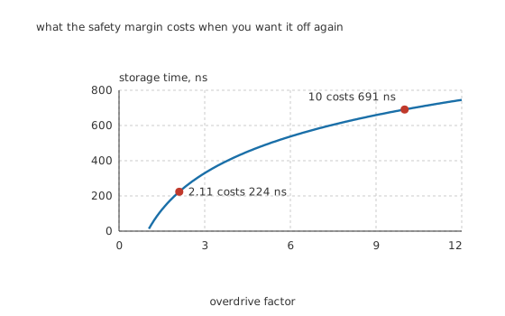
What the safety margin costs when you want it off again.
Worked example — Storage time
In saturation the base is flooded with charge — far more than the collector current needs. Removing the drive does not remove that charge, and until it has gone the collector cannot move.
With a 300 ns time constant, the overdrive of 2.11 costs 224 ns of storage time.
Driving to an overdrive of 10 instead costs 691 ns — only 3.09 times longer for nearly five times the drive, because the dependence is logarithmic.
The logarithm is why the standard practice is what it is. A modest overdrive of two or three is nearly free in time and buys the whole margin; pushing to ten buys very little more certainty and costs three times the delay. The recommendation to design for a forced gain of about a tenth to a fifth of the minimum device gain is that trade, already made.
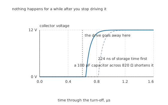
Nothing happens for a while after you stop driving it.
Worked example — The capacitor that shortens it
Put 100 pF across the base resistor. On the falling edge it presents a low impedance for a moment — 82 ns — so the base charge has somewhere to go faster than the resistor alone would allow.
It also helps at turn-on, delivering a burst of extra base current that gets the device into saturation quickly and then letting the resistor take over.
It costs one component and a slightly larger transient load on the driving pin, and it is the standard fix wherever a switched BJT is not fast enough.
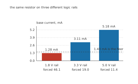
The same resistor on three different logic rails.
Worked example — Why the base resistor is not portable
The same 820 Ω on a 5.0 V rail passes 5.18 mA, a forced gain of 11.4 — even more margin.
On a 1.8 V rail it passes only 1.28 mA, a forced gain of 46.1. That is above the worst-case device gain, so the worst device does not saturate at all.
The junction drop is a fixed subtraction, so a lower rail loses proportionally more of itself to it. A base resistor is a function of the rail it is driven from, and copying one between designs is a real error rather than a stylistic one.
Professional
What it costs to run, and where it stops being the right answer
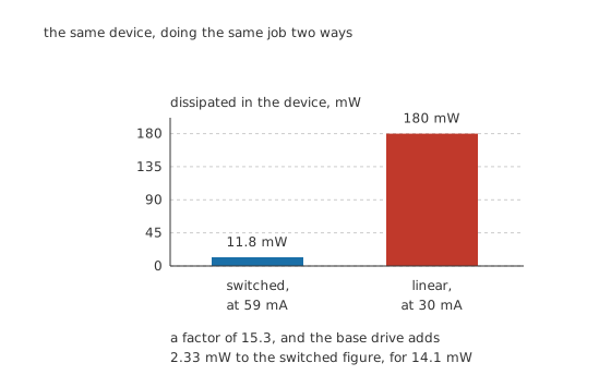
The same device, doing the same job two ways.
Worked example — The dissipation, counted properly
Saturated, the device holds 0.20 V across 59 mA, which is 11.8 mW.
The base drive is not free either: 0.75 V across 3.11 mA is 2.33 mW, bringing the total to 14.1 mW.
Holding the same load at 30 mA with half the supply across the device would cost 180 mW, a factor of 15.3.
The base drive is a fifth of the switched total, which is worth noticing: at low collector currents a bipolar switch's own drive can dominate its losses, and that is one of the arguments for a MOSFET instead.
Four things to settle before the circuit is finished
How the base is turned off. With the drive pin simply released rather than pulled low, the base has no discharge path and the storage time is far worse than calculated. A resistor from base to emitter — a few kilohms — gives the charge somewhere to go and also holds the device off against leakage when nothing is driving it.
Whether the load is inductive. A relay, a solenoid or a motor demands a flyback path, and without one the collector's voltage rises until something breaks down. The flyback diode lesson covers the sizing.
Whether the driver can supply the base current. 3.11 mA is a real load on a logic pin and many cannot supply it. Where the pin cannot, the answer is a driver, a Darlington, or a MOSFET whose gate needs no steady current.
Whether the switch is on the right side of the load. An NPN switching the low side is the arrangement here and the simplest. Switching the high side needs a PNP, or an NPN with a drive referenced above the load — a genuinely different circuit and a common source of trouble.
Where a bipolar switch is still the right choice
Low currents and awkward supplies. Below a few hundred milliamps, a small bipolar transistor and one resistor is cheaper and more forgiving than anything else, and it works from whatever drive voltage is available rather than demanding a defined gate voltage.
Where the drive is a current rather than a voltage. An optocoupler's output, a current-loop signal or another transistor's collector all deliver current, which is exactly what a base wants.
Where speed does not matter. At relay and lamp speeds the storage time is invisible, and every argument for a MOSFET evaporates.
Where it is not: above an amp or two, above a few tens of kilohertz, or where the base drive's own dissipation is a significant fraction of the total. Comparing the two families properly is a lesson of its own.
Common mistakes
- Sizing the base resistor from a typical gain — use the guaranteed minimum. Here 40 at the operating current, not the 150 or 200 a bench measurement might show.
- Reusing a base resistor on a different logic rail — 820 Ω gives 3.11 mA from 3.3 V but only 1.28 mA from 1.8 V, a forced gain of 46.1 which the worst device cannot meet.
- Overdriving as hard as possible — an overdrive of 10 costs 691 ns of storage time against 224 ns at 2.11, and buys nothing the smaller margin did not.
- Releasing the drive pin instead of pulling it low — the base charge then has no discharge path and the storage time is far worse than the calculation suggests.
- Leaving out the flyback diode on an inductive load — the collector's voltage rises until something breaks down, and the something is usually the transistor.
- Forgetting the base drive in the dissipation — 2.33 mW here against 11.8 mW in the channel, which is a fifth of the total.
Parts used in this topic
Frequently asked questions
How do I choose the base resistor for a switch?
Work out the load current, divide by the guaranteed minimum gain to get the base current the worst device needs, then supply several times it. Here 59 mA through 200 Ω needs 1.48 mA at a minimum gain of 40, and 820 Ω from a 3.3 V pin supplies 3.11 mA — an overdrive of 2.11.
What is forced gain and what should it be?
The load current divided by the base current actually supplied — 19.0 here. It should be comfortably below the device's guaranteed minimum gain, typically a fifth to a tenth of it, so that even the worst device saturates.
Why does overdriving make turn-off slower?
Because saturation floods the base with charge, and that charge has to be removed before the collector can move. The delay follows the logarithm of the overdrive: 224 ns at an overdrive of 2.11, and 691 ns at 10. The logarithm is why a modest margin is nearly free and a large one is not worth buying.
Does the base drive matter to the power budget?
More than people expect at low currents. Here the channel loses 11.8 mW and the base drive 2.33 mW, for 14.1 mW total — the drive is a fifth of it. A MOSFET's gate needs no steady current at all, which is one of the arguments for using one instead.
Can I use the same circuit on a different supply rail?
Not without recalculating. The junction's 0.75 V is a fixed subtraction, so a lower rail loses proportionally more of itself to it. The same 820 Ω gives 5.18 mA from 5.0 V and only 1.28 mA from 1.8 V, and the last of those does not saturate the worst device.
Knowledge check
Design the base resistor for a 200 Ω load on 12 V driven from a 3.3 V pin, with a minimum gain of 40. (Show answer)
What does the overdrive cost at turn-off? (Show answer)
What does the same 820 Ω resistor do on 1.8 V and 5.0 V rails? (Show answer)
Compare what the device dissipates switched against holding the same load linearly. (Show answer)
Which way round does the flyback diode go, and when does it conduct? (Show answer)
One email a month from the bench
New circuits, lessons, part guides and calculators, on the first Sunday of each month.