
Quick Answer
A transistor's current gain is the ratio of collector current to base current. It is specified as a range rather than a value, it peaks at some mid-range current and falls off either side, and it climbs with temperature — so a circuit that depends on knowing it is a circuit that will not repeat.
Intuition
Rated to hold at least this much
Why does a steel bolt carry a grade stamped on its head rather than a measured strength? Nobody publishes what any particular bolt will actually take, because the answer varies from bolt to bolt, changes with the batch and depends on how it is loaded. What the stamp promises is a floor: at least this much, in these conditions.
Current gain is sold the same way, and read the same way. The datasheet gives a minimum and often a maximum, at one stated current and one stated temperature, and everything outside that one point is somebody else's problem.
Three things move it, and they multiply rather than replace one another.
Part to part. Two devices from the same reel can differ by a factor of three. This is not a defect — it is what the manufacturing spread is, and the factory sorts devices into bins to sell the tighter ones at a premium.
With current. Gain peaks somewhere in the middle of the device's useful range and falls away at both ends, steeply at the bottom and steadily at the top.
With temperature. It climbs as the device warms, by enough that a cold morning and a hot enclosure are two different transistors.
The conclusion that follows is the useful part of this lesson, and it is not "measure it". It is to build circuits whose behaviour does not depend on it. A good design treats gain the way a good structure treats a bolt's grade: check there is enough, and then arrange not to care exactly how much.
Practitioner
The band, and what the datasheet is promising
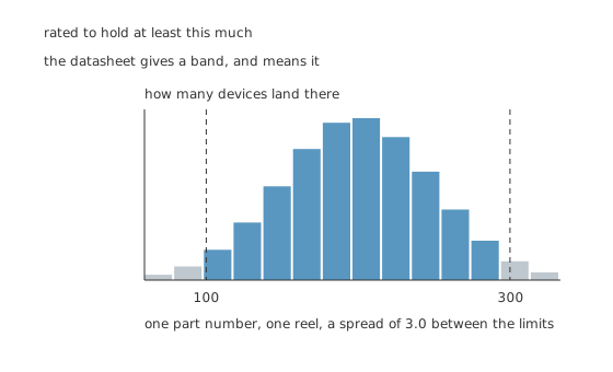
The datasheet gives a band, and means it.
Worked example — What a specification actually says
A part specified from 100 to 300 covers a spread of 3.0.
Both ends are real devices that will arrive in real reels. The manufacturer guarantees only that no device falls outside the band, at the one current and the one temperature the specification names.
Nothing in that promise is about the device in front of you. Measuring one tells you about one, and the next board gets a different one.
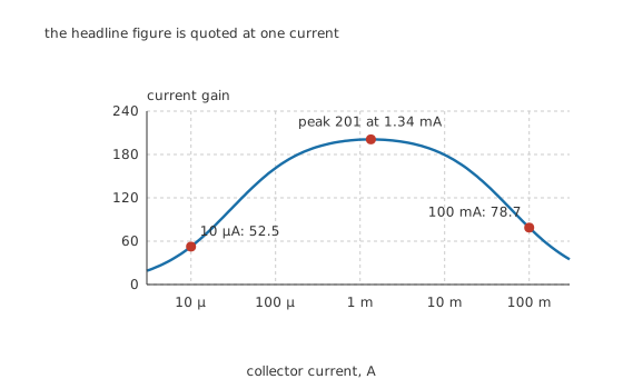
The headline figure is quoted at one current.
Worked example — What running at a different current costs
This device peaks at 201 at 1.34 mA, and at the nominal 1.0 mA it gives 201.
Run the same device at 10 µA and the gain falls to 52.5 — a factor of 3.82, from the current alone.
Run it at 100 mA and it falls again, to 78.7, as high-level injection sets in.
The two roll-offs have different causes. At the bottom, recombination in the emitter-base depletion region takes a fraction of the base current that does not scale with the collector current. At the top, the injected carrier density approaches the base's own doping and the base stops behaving as a lightly doped layer at all.
Engineer
Temperature, and the two different gains
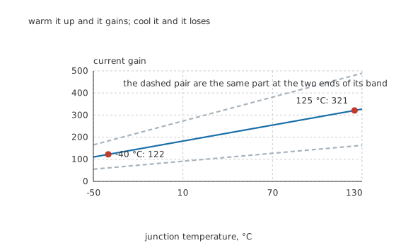
Warm it up and it gains; cool it and it loses.
Worked example — What a working temperature range does
Gain rises at about 6.0 m per degree, so the device that gives 201 at 25 °C gives 122 at -40 °C and 321 at 125 °C.
That is a ratio of 2.62 from one device, before any part-to-part spread has been considered.
The rise is a consequence of the base transport factor improving as carriers gain thermal energy, and it is one of the mechanisms behind thermal runaway: more heat means more gain, more gain means more current, more current means more heat.
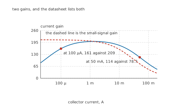
Two gains, and the datasheet lists both.
Worked example — Why there are two gains and when they differ
The DC gain is collector current divided by base current. The small-signal gain is the slope — how much the collector current changes for a small change in base current.
Where the gain curve is rising, the slope is steeper than the ratio: at 100 µA the DC gain is 161 while the small-signal gain is 209.
Where it is falling, the slope is shallower: at 50 mA the DC gain is 114 and the small-signal gain only 78.7, a ratio of 0.688.
At 1.0 mA, near the peak, they are 201 and 203 — close enough to use interchangeably, which is why the distinction is usually ignored and why it bites at the extremes.
Professional
What to do about it
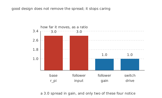
Good design does not remove the spread; it stops caring.
Worked example — Two quantities that move, and two that do not
At 1.0 mA the transconductance is 38.7 mS, which the gain has no say in at all.
The base's own input resistance moves fully, from 2.59 kΩ to 7.76 kΩ, and so does an emitter follower's, from 50 kΩ to 150 kΩ driving 500 Ω.
A follower's voltage gain does not move at all. With 1.0 kΩ in the emitter driving a 1.0 kΩ load, it is that combined load divided by the load plus 25.9 Ω, which is 0.951 whatever device is fitted, because the gain cancels out of the expression.
Nor does a saturated switch's base current. Driving 10 mA at a forced gain of 20 needs 500 µA, and that number came from a choice rather than from the device.
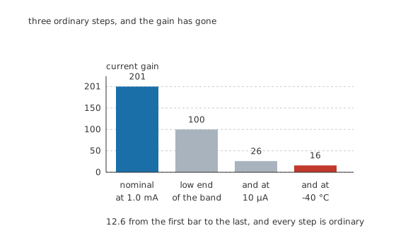
Three ordinary steps, and the gain has gone.
Worked example — Stacking the three effects
Start at 201 — a nominal device at 1.0 mA and 25 °C.
Take a device at the low end of the band. Then run the circuit at 10 µA rather than at the nominal current. Then cool it to -40 °C.
What is left is 16.0, which is 12.6 below the bench figure. None of the three steps is unusual, and a design that assumed the bench figure has no margin left at all.
The four techniques that remove the dependence
Set current with an emitter resistor. Divider bias turns a base voltage into an emitter current, and the gain appears only in a small correction term. That is why it is the standard arrangement.
Design a switch to a forced gain. Choose a ratio well below the worst-case device gain — a fifth or a tenth — and the base drive becomes a decision rather than a consequence. The switch lesson works that through.
Use negative feedback around the stage. Any feedback loop with plenty of open-loop gain sets its closed-loop behaviour from its passive components, and a factor of three in device gain becomes a fraction of a per cent at the output.
Buy the gain twice over where it genuinely matters. A Darlington pair multiplies two gains together, which turns a worst case of sixteen into a worst case of hundreds, at the cost of a second junction drop and much worse saturation.
Two places the number is genuinely needed
Checking a driver can supply the base current. This is a worst-case calculation, and it wants the minimum gain at the operating current and the lowest temperature. That is what the stack above is for.
Estimating a stage's input resistance. This one has no fix. The base's input resistance is proportional to the gain, so a stage whose input resistance matters will have an input resistance that varies by whatever the gain does — and the answer is to make the bias divider, not the base, dominate it.
Common mistakes
- Designing to a measured gain — the device measured is not the device that arrives on the next board. Use the datasheet's minimum, at your current and your temperature.
- Assuming the headline figure applies at your operating current — it is quoted near the peak. At 10 µA this device gives 52.5 rather than 201, a factor of 3.82 from the current alone.
- Forgetting temperature — the same device gives 122 at −40 °C and 321 at 125 °C, a ratio of 2.62 before any part spread.
- Confusing the DC gain with the small-signal gain — they agree near the peak and diverge at the extremes, reaching a ratio of 0.688 at 50 mA on this device.
- Stacking the worst cases without noticing — low-band part, low current and low temperature together leave 16, which is 12.6 below the bench figure.
- Trying to solve the spread by measuring and sorting — that is a manufacturing cost with no end. Design so the gain cancels instead.
Frequently asked questions
Why is current gain specified as a range?
Because that is what manufacturing produces. A three-to-one spread from 100 to 300 across one part number is ordinary, and the factory sorts devices into bins rather than making them identical. The specification is a promise about the band, at one stated current and temperature, and about nothing else.
How much does gain change with operating current?
A great deal at the extremes. This device peaks at 201 near 1.34 mA, falls to 52.5 at 10 µA and to 78.7 at 100 mA. The low-current fall is depletion-region recombination; the high-current fall is high-level injection, where the injected carriers rival the base's own doping.
What is the difference between hFE and hfe?
The capitals are the DC gain — collector current divided by base current. The lower case is the small-signal gain, which is the slope of that curve. Where the curve rises they differ one way and where it falls the other: 161 against 209 at 100 µA, and 114 against 78.7 at 50 mA. They agree at the peak, where the slope is zero.
Does gain go up or down with temperature?
Up, at roughly 6.0 m per degree. A device giving 201 at 25 °C gives 122 at −40 °C and 321 at 125 °C. That rise is one of the mechanisms behind thermal runaway, since more heat gives more gain gives more current gives more heat.
If gain varies so much, how does anything work?
Because good circuits are arranged so it cancels. An emitter follower's voltage gain is 0.951 whatever device is fitted; a saturated switch's base current of 500 µA came from a chosen forced gain rather than the device's own. The quantities that do move — the base's input resistance, from 2.59 kΩ to 7.76 kΩ — are usually swamped deliberately by something that does not.