
Forward biasing the base-emitter junction injects carriers into the base, and the reverse-biased collector junction sweeps up almost all of them. The collector current follows the base-emitter voltage exponentially, and the base current is only the small fraction that never completes the crossing.
Intuition
Only the first step needs pushing
Getting a heavy trolley over a doorstep takes effort. Getting it down the ramp on the other side takes none: once it is over the lip, gravity does the rest, and how far it runs is decided by how many trolleys you pushed over, not by how steep the ramp is.
A transistor's two junctions are that doorstep and that ramp. The base-emitter junction is the step: it has to be pushed, and pushing it costs voltage. The base-collector junction is the ramp, and it is doing the opposite of blocking — it is reverse biased, which means its field is pulling hard in exactly the direction the arriving carriers are already going.
So the two junctions are not two obstacles in series. One of them decides how much traffic starts, and the other collects whatever arrives. The base is only wide enough to be crossed, and the crossing takes almost nothing away.
That division is why one small voltage at the base-emitter junction controls a large current at the collector, and why raising the collector's voltage further does very little. The ramp is already steep enough. Adding to it does not increase the number of trolleys somebody pushed over the step.
Practitioner
Forward at one end, reverse at the other
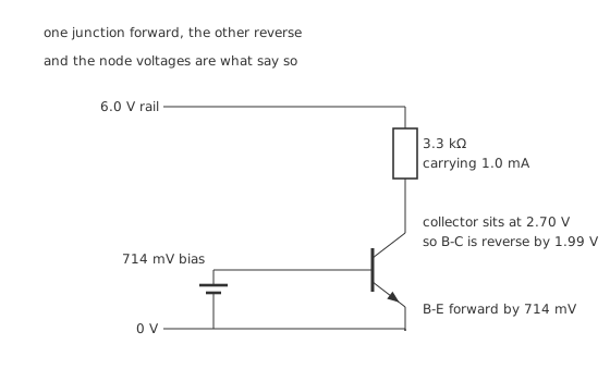
The node voltages, not the labels, are what say which junction is which way.
The condition is worth stating flatly, because the whole department depends on it. Base-emitter forward biased, base-collector reverse biased. That pair of senses is what "active region" means, and any circuit that fails to arrange it gets something other than amplification.
Worked example — The bias the circuit actually establishes
At 300 K the thermal voltage is 25.9 mV, which sets the scale for everything the junction does.
Hold the base 714 mV above the emitter and the collector carries 1.0 mA. Dropping that through 3.3 kΩ from a 6.0 V rail leaves the collector at 2.70 V.
The base-collector junction therefore has 1.99 V across it in reverse, and the device is properly in its active region.
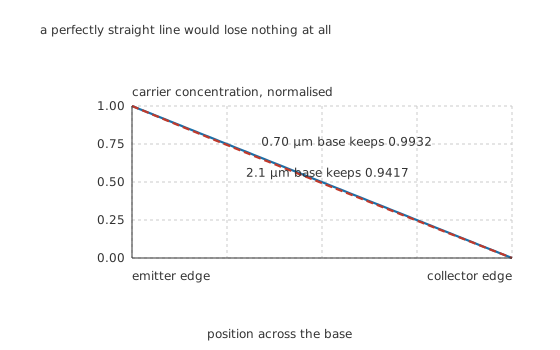
The sag in the curve is the recombination, drawn.
Inside the base, the carriers are not being pushed by a field — they are diffusing, sliding down a concentration gradient from a crowded emitter edge to a collector edge the field keeps swept clear. A straight-line gradient would mean nothing was lost on the way. What the profile actually does is sag slightly, and the size of that sag is exactly the fraction that recombines.
Engineer
The exponential, and the sixty millivolts that come with it
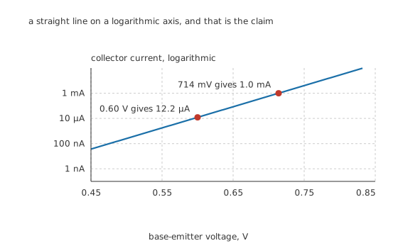
A straight line on a logarithmic axis is the claim being made.
The base-emitter junction obeys the same law any forward-biased junction does, so the collector current is exponential in the base-emitter voltage. The consequence practitioners actually use is the slope of that exponential.
Worked example — What a decade of current costs in millivolts
At 25.9 mV, multiplying the current by ten takes 59.5 mV of extra base-emitter voltage. Nothing about the device enters that number except its temperature.
So 1.0 mA at 714 mV becomes 10 mA at 774 mV, a gap of 59.5 mV.
Over a wider span the same rule holds: 0.60 V gives 12.2 µA and 0.70 V gives 582 µA, a factor of 47.9 for a hundred millivolts.
The saturation current that anchors that exponential is a very small number — several decades below a picoamp for a small-signal device — which is why the lesson works from a measured point on the curve rather than from the constant itself. One current at one voltage plus the sixty-millivolt rule reproduces the whole characteristic, and it is far easier to measure.
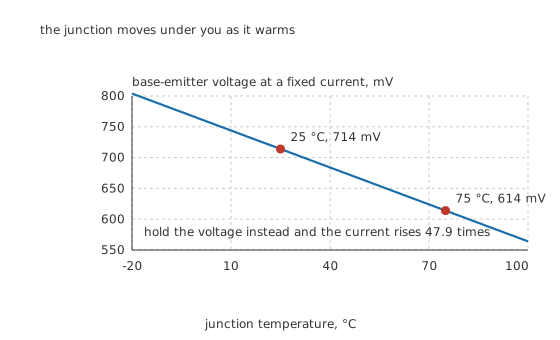
Held at a fixed voltage instead, the same warming multiplies the current by 47.9.
Worked example — Why a transistor is never biased from a voltage alone
Hold the collector current at 1.0 mA and the base-emitter voltage falls by about -2.0 mV per degree, so a 50 °C rise takes 714 mV down to 614 mV.
Now do it the other way round. Hold the base-emitter voltage fixed at 714 mV and let the device warm by the same 50 °C. The curve has moved 1.68 decades to the left underneath it, so the current climbs by a factor of 47.9.
That is the same device, the same warming, and two completely different outcomes, and it is the whole reason biasing is a topic at all.
Professional
What sets the gain, and what sets the speed
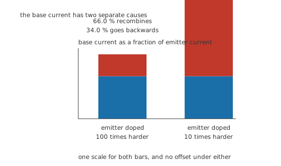
Two separate leaks, and only one of them is about the base.
Base current has two causes, and treating it as one number hides which of them a given device is limited by.
Worked example — The two leaks, sized against each other
With the base 0.70 µm across and a 6.0 µm diffusion length, 0.9932 of what enters survives the crossing. The rest recombines.
Separately, some charge travels the wrong way — out of the base back into the emitter. With the emitter doped 100 times harder than the base across a 2.0 µm emitter, that leak leaves 0.9965 of the traffic going the right way.
Multiply the two and the device passes 0.9898 of its emitter current to the collector, a gain of 96.7. Of the base current that remains, 66.0 % is recombination and 34.0 % is back-injection.
Drop the emitter's doping advantage to 10 and the injection term collapses to 0.9662, at which point back-injection dominates and the base's thinness stops mattering. A heavily doped emitter is not an optimisation; without it the geometry buys nothing.
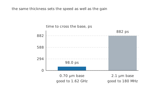
The same dimension that sets the gain sets the ceiling on frequency.
Worked example — How long the crossing takes
Diffusion across the base takes a time that follows the square of the width. At a diffusion constant of 25 square centimetres per second, the 0.70 µm base is crossed in 98.0 ps, which puts a ceiling of 1.62 GHz on the device.
The 2.1 µm base takes 882 ps and falls to 180 MHz, a factor of 9.00.
Because the dependence is on the square rather than the width itself, the speed penalty is larger than the gain penalty for the same change.
Three places this model stops describing the device
Above a certain current density, the gain falls off. Injected charge eventually becomes comparable to the base's own doping, and past that point pushing more current in stops raising the collector current proportionally. The exponential still applies to the junction; the ratio no longer applies to the device.
At low current, recombination in the depletion region takes over. That is a different mechanism with a different slope, so the straight line on the logarithmic axis bends at the bottom and the effective ideality drifts above 1.0.
The base width is not a constant. Raising the collector-emitter voltage widens the base-collector depletion region, which eats into the base and thins it, which raises the gain a little. That is the Early effect, and it is why the small-signal model has to give the collector a finite output resistance rather than treating it as a perfect current source.
Where this leaves a practitioner
Think in currents, design in currents. The exponential is real, but it is far too steep and far too temperature-dependent to design against directly. Every practical circuit sets a current and lets the base-emitter voltage land wherever it lands. The operating regions lesson is where that becomes a procedure.
The two-millivolt slope is a tool, not only a nuisance. A junction whose forward voltage tracks temperature that predictably makes a serviceable thermometer, and it is what lets a current mirror hold its ratio while the chip it sits on warms up.
Common mistakes
- Reading the two junctions as two diodes in series — a transistor tested that way looks like two diodes, but the behaviour depends on the base being thin enough for one junction's carriers to reach the other. Two separate diodes wired base to base amplify nothing.
- Biasing the base from a fixed voltage — the curve moves about 2.0 mV per degree, so a 50 °C rise at a fixed 714 mV multiplies the collector current by 47.9. Bias sets a current, never a voltage.
- Quoting a single base-emitter voltage for the device — it is 714 mV at 1.0 mA and 774 mV at 10 mA on this junction. The voltage is a consequence of the current you chose.
- Expecting more collector voltage to give more collector current — the base-collector junction is already reverse biased and already collecting everything that arrives. Extra voltage there changes almost nothing.
- Assuming a thin base is the only requirement for gain — with the emitter doped only 10 times harder than the base, injection efficiency falls to 0.9662 and back-injection dominates the base current whatever the base width is.
Frequently asked questions
Why is the collector junction reverse biased when the device is supposed to be conducting?
Because it is not conducting in the ordinary sense. Its reverse field is what sweeps up carriers arriving from the base, and a reverse-biased junction does that better than a forward-biased one. Current flows through it only because the base keeps delivering carriers to its edge, not because the junction has been persuaded to conduct.
What is the 60 mV rule and where does it come from?
It is the extra base-emitter voltage that multiplies the collector current by ten. At 300 K it works out at 59.5 mV, and it comes from the thermal voltage of 25.9 mV multiplied by the natural logarithm of ten. Nothing about the transistor enters it except the temperature.
How much does base-emitter voltage move with temperature?
About 2.0 mV per degree downwards at a fixed current, so 714 mV at 25 °C becomes 614 mV at 75 °C. Run the same experiment at a fixed voltage instead and the current climbs 47.9 times over the same rise, which is the version that destroys circuits.
Why does the emitter have to be doped so much more heavily than the base?
Because carriers cross the base-emitter junction in both directions, and only one of those directions is useful. Doping the emitter 100 times harder makes the useful direction 0.9965 of the traffic. Drop that ratio to 10 and it falls to 0.9662, at which point the wrong-way current dominates the base current and the gain collapses regardless of how thin the base is.
Does the thin base help with speed as well as gain?
Yes, and more so. Transit time follows the square of the base width, so the 0.70 µm base crosses in 98.0 ps against 882 ps for 2.1 µm — a factor of 9.00 in usable frequency, against a factor of about nine in gain for the same change.
Knowledge check
What bias condition puts a BJT in its active region, and how would you check it from node voltages? (Show answer)
How much extra base-emitter voltage multiplies the collector current by ten? (Show answer)
A transistor biased at a fixed base-emitter voltage warms by 50 °C. What happens to its collector current? (Show answer)
What two separate losses make up the base current, and how big is each here? (Show answer)
How does base width affect the highest frequency the device is good for? (Show answer)
One email a month from the bench
New circuits, lessons, part guides and calculators, on the first Sunday of each month.