
Quick Answer
A small-signal model replaces a transistor with linear elements valid for small changes about a chosen operating point. The hybrid-pi version uses three: an input resistance at the base, a current source set by the base-emitter signal, and an output resistance at the collector.
Intuition
A local map, drawn where you are standing
Why is a street map of one neighbourhood drawn flat? The earth is not, and nobody minds, because over a few hundred metres the curvature is smaller than the ink. Walk far enough and the flat map stops working — but for the walk you are actually taking, it is exact enough and far easier to use than a globe.
A transistor's behaviour is a curve, and curves are hard to calculate with. The small-signal model is the flat map: pick the operating point the circuit will sit at, work out the slope of the curve there, and treat the device as though that slope were the whole story.
Everything the model does follows from that. It says nothing about where the operating point is — that was decided by the bias network before the model was drawn. It says nothing about clipping, because a straight line has no ends. And it is accurate only while the signal is small enough that the curve has not visibly bent, which is a stricter condition than most people expect.
What you get in exchange is that the transistor disappears. In its place are three ordinary linear components, and the circuit around them can be solved with nothing more than Ohm's law and the rules for series and parallel. A stage that was a nonlinear device with a supply rail becomes a network of resistors and one dependent source, and that is the whole reason the model is worth learning.
Practitioner
Three elements, and where each comes from
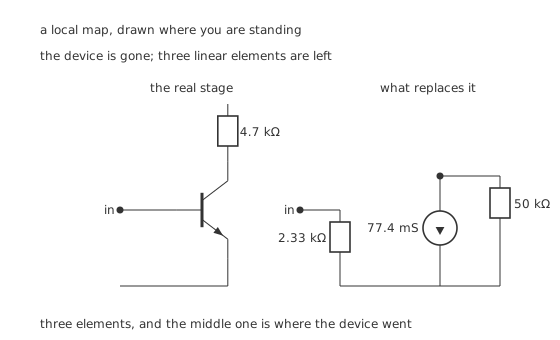
The device is gone; three linear elements are left.
Worked example — All three, from one bias current
Bias the device at 2.0 mA. At 300 K the thermal voltage is 25.9 mV, so the transconductance is 77.4 mS.
The current gain of 180 divided by that gives the base's input resistance, 2.33 kΩ.
An Early voltage of 100 V divided by the bias current gives the collector's output resistance, 50 kΩ.
Looking into the emitter rather than the base, the device offers only 12.9 Ω, which is one over the transconductance — the same fact stated from the other terminal.
Each element corresponds to something physical. The transconductance is the slope of the exponential at the chosen current. The input resistance exists because the base takes current — a device with infinite gain would have an infinite one, and a MOSFET's is effectively that. The output resistance is the tilt of the output curves, which is why it appears here as a resistance rather than as a perfect current source.
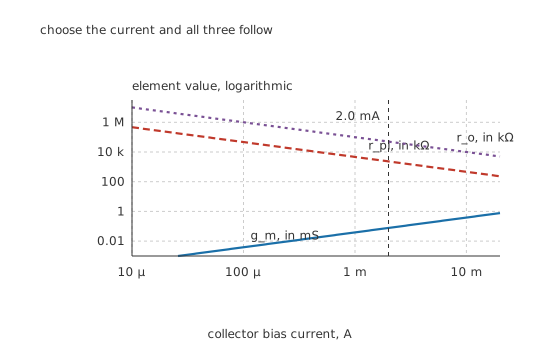
Choose the current and all three follow.
Notice what that figure says about design freedom. Only one number is chosen — the bias current — and the other three are consequences. Wanting more transconductance means running more current, which lowers both resistances at the same time, and there is no way to have one without the others.
Engineer
What the model predicts, and the ceiling it reveals
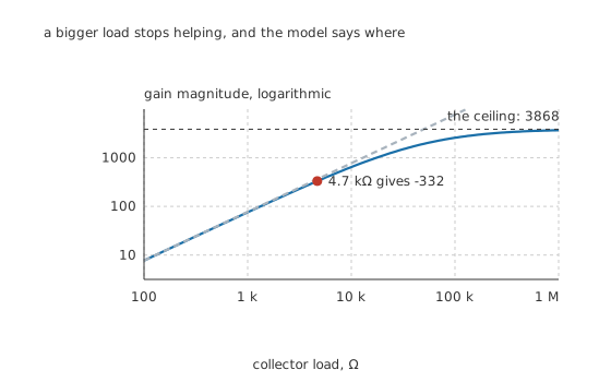
A bigger load stops helping, and the model says where.
Worked example — A stage's gain, done properly
The collector drives 4.7 kΩ, but the device's own 50 kΩ is in parallel with it, so the real load is 4.30 kΩ.
The gain is therefore -332, against the -364 the collector resistor alone would suggest — a difference of 8.59 %.
At this load the correction is small enough to be a refinement. Raise the load and it stops being one.
Worked example — The gain a single stage cannot exceed
Push the collector load higher and higher and the gain approaches the transconductance multiplied by the output resistance alone: 3868.
Now do the algebra rather than the arithmetic. The transconductance is the current divided by the thermal voltage, and the output resistance is the Early voltage divided by the same current. The current cancels. The ceiling is the Early voltage divided by the thermal voltage, and it is the same at every bias point.
That number — called the intrinsic gain — is a property of the device and its temperature, and nothing a circuit designer does to the load can beat it.
That result explains a piece of practice that otherwise looks like showing off. An integrated amplifier replaces the collector resistor with a current mirror, whose resistance is very large, precisely to get as close to the intrinsic gain as possible. A resistor-loaded stage cannot, because a resistor large enough would also drop the whole supply.
Professional
Where the model stops being true
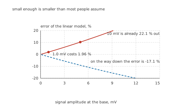
Small enough is smaller than most people assume.
Worked example — How small the signal has to be
Compare the model's straight line with the exponential it approximates, at the base.
At 1.0 mV the model is 1.96 % out. At 5.0 mV it is 10.3 % out. At 10 mV it is 22.1 % out on the positive half and -17.1 % on the negative one.
The asymmetry is the important part. A model that is wrong by the same amount in both directions would only mis-scale the output; one that is wrong by different amounts produces a second harmonic, which is exactly the distortion the common-emitter lesson measures.
So "small signal" means a millivolt or two at the base for a few per cent accuracy, not the ten or twenty most people picture.
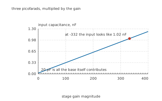
Three picofarads, multiplied by the gain.
Worked example — The capacitance the model has to add back
The base-to-collector capacitance is tiny — 3.0 pF. But its two ends move in opposite directions, and the collector end moves -332 times as far, so the charge the source has to supply is as if the capacitance were multiplied by one plus the gain.
That multiplied term is 1.00 nF, and with the base's own 20 pF the input looks like 1.02 nF.
Against a 1.0 kΩ source that puts the corner at 156 kHz, where the base capacitance alone would have allowed 7.96 MHz.
A factor of 51.0 in bandwidth, paid for the gain — and the reason the cascode exists.
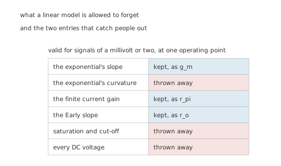
What a linear model is allowed to forget.
Three ways the model misleads people who trust it
It will predict an output larger than the supply. There are no rails in a small-signal circuit, so nothing stops the algebra. A stage whose model says it produces forty volts of output from a twelve-volt supply is being described correctly by a model that was never told the supply exists.
It says nothing about the operating point it depends on. Every element in it was computed from the bias current, so a bias that has drifted with temperature has changed the model without changing the drawing. A 7 % shift in bias is a 7 % shift in transconductance and therefore in gain.
It is a single-frequency picture unless capacitances are added. The three-element version has no frequency response at all. Adding the two capacitances above gives it one, and adding them is not optional for anything faster than audio.
Where this model is used next
The hybrid-pi elements are the vocabulary the rest of the department works in. The differential pair is two of these models sharing a tail; the current mirror is valued for the size of its output resistance; and an emitter follower's impedance transformation is a two-line result once the model is in place. The same three elements, arranged differently, describe every one of them.
The MOSFET version is the same shape with one element removed: no gate current means no input resistance at all, and the model reduces to a transconductance and an output resistance. Everything else transfers unchanged.
Common mistakes
- Using the model on signals that are not small — at 10 mV at the base it is already 22.1 % out on one half of the cycle and −17.1 % on the other, which is not an approximation, it is a different answer.
- Forgetting r_o in the load — at 4.7 kΩ it costs 8.59 % of the gain, and as the collector load rises it becomes the limit rather than a correction.
- Believing a gain the model predicts without checking the supply — small-signal circuits have no rails, so nothing in the algebra prevents an output larger than the supply that feeds it.
- Treating the model as fixed — every element came from the bias current, so a bias that drifts takes the model with it.
- Ignoring the multiplied base-to-collector capacitance — 3.0 pF becomes 1.00 nF at a gain of 332, which costs a factor of 51.0 in bandwidth.
Frequently asked questions
What are the three elements and where do they come from?
An input resistance from base to emitter, a current source driving the collector from the base-emitter signal, and an output resistance from collector to emitter. At 2.0 mA they are 2.33 kΩ, 77.4 mS and 50 kΩ. All three come from the bias current, so choosing that one number fixes the other three.
How small does a small signal have to be?
Smaller than most people assume. At the base, 1.0 mV gives a 1.96 % error, 5.0 mV gives 10.3 %, and 10 mV gives 22.1 % on one half and −17.1 % on the other. For a few per cent accuracy the answer is a millivolt or two.
Why does the gain stop rising as the collector load increases?
Because the device's own output resistance is in parallel with the load, so the total can never exceed it. The ceiling is the transconductance multiplied by the output resistance, 3868 here — and since the bias current cancels out of that product, it is the Early voltage divided by the thermal voltage and is the same at every bias point.
Why does the model not have a supply rail in it?
Because a small-signal model describes changes, and a fixed supply does not change. That is convenient for the algebra and dangerous for the conclusions: the model will happily predict an output swing larger than the supply, because nothing in it knows the supply exists.
Does the same model work for MOSFETs?
Yes, with one element removed. No gate current means no input resistance, so the model reduces to a transconductance and an output resistance. Everything about how the elements combine into gains and impedances transfers unchanged.