
A differential pair is two matched transistors whose emitters share one current source. Because that tail total is fixed, current can only move from one side to the other, so the pair amplifies the difference between its two inputs and largely ignores whatever they do together.
Intuition
Both microphones hear the room; only one hears the voice
Set two microphones side by side and one of them next to a speaker. Both pick up the traffic outside, the air conditioning and the hum from the lights, in almost equal measure. Only one picks up the voice. Subtract one signal from the other and the room cancels while the voice survives.
A differential pair does that subtraction in hardware, and it does it through one constraint. The two transistors share a single current source at their emitters, and that source's total does not change. Whatever one device stops carrying, the other has to start carrying, because there is nowhere else for the current to go.
Push one base up and the other down and the imbalance is large: current pours from one side to the other. Push both bases up together and nothing happens at all, because the total was fixed before either input moved.
That single arrangement is behind more circuits than almost any other. Every operational amplifier's input stage is one. Every comparator is one. Every balanced audio input, every instrumentation amplifier, every long-tailed pair in an old valve schematic — all the same idea, and all relying on the same fixed tail.
The properties it gives away are worth naming too. It is only linear over a few tens of millivolts, its rejection of common signals is only as good as its tail current source, and any mismatch between the two devices is indistinguishable from a real input.
Practitioner
The circuit, and the node that makes it work
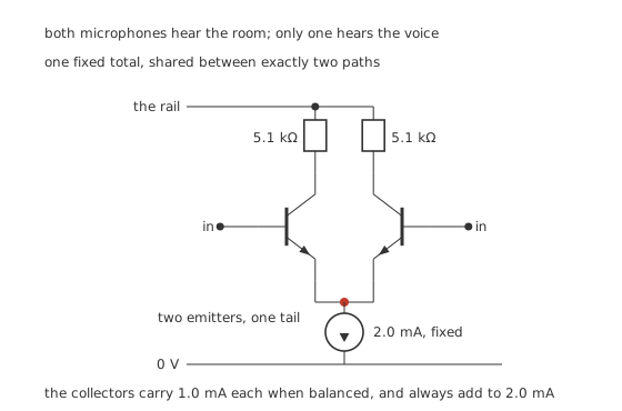
One fixed total, shared between exactly two paths.
Worked example — The bias, and the gain it produces
A 2.0 mA tail splits equally when the inputs match, so each device carries 1.0 mA.
At 25.9 mV that gives each device a transconductance of 38.7 mS.
Taking the output from one collector, the differential gain is that transconductance multiplied by 5.1 kΩ: 197, or 45.9 dB.
The node to check on any schematic is the tail. Exactly two emitters and one current source meet there, and nothing else. If either emitter goes to ground separately, the circuit is two ordinary common-emitter stages that happen to share a supply — and everything in this lesson stops being true of it.
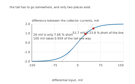
The tail has to go somewhere, and only two places exist.
Worked example — How far the straight line goes
The tail divides according to the ratio of two exponentials, which is a hyperbolic tangent — and near the origin a hyperbolic tangent is a straight line.
At 26 mV of differential input the real curve is already 7.66 % below the straight line. At 51.7 mV it is 23.8 % below.
By 100 mV the curve has flattened and 0.959 of the whole tail has moved to one side.
Both halves of that are useful. As an amplifier the pair is linear over a few tens of millivolts and no more. As a comparator, the same flattening is exactly what is wanted: a hundred millivolts of input and the tail has gone entirely one way.
Engineer
What it rejects, and what decides how well
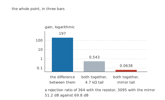
The whole point, in three bars.
Worked example — Why a common signal produces anything at all
In principle both inputs rising together changes nothing. In practice it does, because a real tail is not a perfect current source.
With a plain resistor of 4.7 kΩ as the tail, raising both inputs raises the tail node too, which raises the current through that resistor, which raises both collector currents. The common-mode gain works out at 0.543, and the rejection ratio at 364 — 51.2 dB.
Replace the resistor with a current mirror, whose output resistance is 40 kΩ, and the common-mode gain falls to 0.0638. The rejection rises to 3095 — 69.8 dB, an improvement of 18.6 dB.
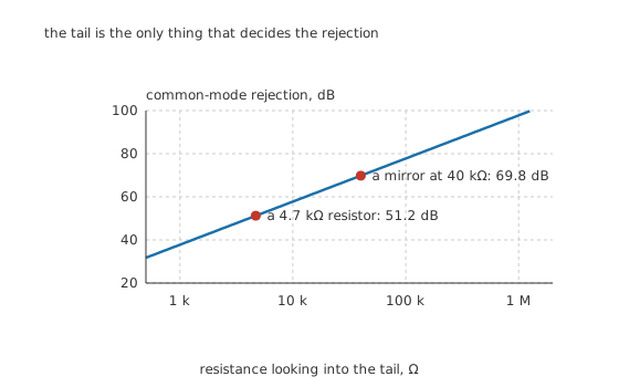
The tail is the only thing that decides the rejection.
No other component in the circuit moves it. Better-matched devices improve the offset; larger collector resistors raise both gains equally and change the ratio not at all. Only the tail's resistance moves the rejection, and a current source is the only practical way to make it large without dropping the supply across it.
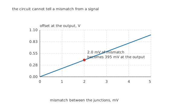
The circuit cannot tell a mismatch from a signal.
Worked example — The error the circuit is blind to
A difference of 2.0 mV between the two junctions is indistinguishable, to the pair, from 2.0 mV of real input.
Multiplied by the gain, it appears at the output as 395 mV.
That is the same two millivolts that costs a current mirror eight per cent of its accuracy, and for the same reason: the exponential turns millivolts into large effects. Matched devices, on one die, at one temperature, are not an optimisation here.
Professional
The active load, and where the arrangement leads
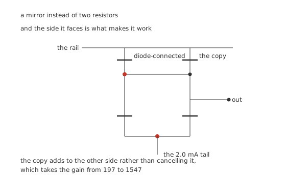
A mirror instead of two resistors, and the side it faces is what makes it work.
Worked example — What replacing the resistors buys
A resistor load has to drop DC voltage to present AC resistance, and the supply limits how much. A mirror presents its own output resistance instead: at an Early voltage of 80 V and 1.0 mA per side, that is 80 kΩ — and it drops almost nothing.
The gain rises from 197 to 1547, a factor of 7.84.
And it does a second job for free. The mirror copies the current from the inverting side across to the output side, where it adds to what that side is doing — so the pair's two-sided output becomes one single-ended output with no loss of signal.
The orientation is the part to check. The diode-connected half of the mirror must face the device carrying the inverted half of the signal. Reversed, the copy subtracts instead of adding and the stage has no gain at all — while looking entirely reasonable on the schematic.
Four things that follow from the arrangement
The input range is limited at both ends. The tail source needs some voltage across it, so the inputs cannot go too low; the collector resistors' drop limits how high they can go before a device saturates. Between those is the common-mode input range, and it is a specification worth reading on any real amplifier.
Emitter degeneration widens the linear range and costs gain. Resistors in both emitters extend the straight part of the transfer characteristic and reduce the gain by the same factor, exactly as they do in a common-emitter stage. Where the pair has to handle more than a few tens of millivolts, that is the standard cure.
The tail current sets everything at once. Transconductance, gain, input resistance, noise and speed all follow from it, and there is only one of it to choose. That is the same one-degree-of-freedom situation the small-signal model describes.
MOSFET pairs behave identically in structure and differently in detail. The tail constraint is the same, the mirror load is the same, and the transfer characteristic follows the square law rather than the exponential, which makes the linear range wider and the gain lower.
Where this leads
An operational amplifier is, at its input, exactly this circuit: a differential pair with a mirror tail and a mirror load, feeding a high-gain stage and then an output buffer. Every property this lesson computes — the input offset, the common-mode rejection, the limited input range, the modest linear range — appears on that amplifier's datasheet as a specification, and now has a mechanism attached to it.
The comparator is the same circuit with the linearity deliberately abandoned: drive it past a hundred millivolts and the tail commits entirely to one side, which is a decision rather than an amplification.
Common mistakes
- Grounding one emitter separately — the shared tail is the whole mechanism. With separate emitter returns the circuit is two common-emitter stages and none of its differential properties hold.
- Expecting linearity beyond a few tens of millivolts — at 26 mV the transfer characteristic is already 7.66 % below the straight line, and at 51.7 mV it is 23.8 % below.
- Improving the rejection by matching devices better — matching fixes the offset. Only the tail's resistance moves the rejection: 51.2 dB with a 4.7 kΩ resistor against 69.8 dB with a mirror.
- Ignoring input offset — 2.0 mV of junction mismatch is indistinguishable from a real 2.0 mV input and appears as 395 mV at the output.
- Reversing the mirror load — the diode-connected half must face the inverting device so the copy adds. Reversed it subtracts, the gain collapses, and the schematic still looks correct.
- Forgetting the common-mode input range — the tail source needs headroom below and the collector resistors' drop limits the top.
Frequently asked questions
How linear is a differential pair?
Over a few tens of millivolts. The tail divides as a hyperbolic tangent, which is straight near the origin and bends quickly: 7.66 % below the line at 26 mV and 23.8 % below at 51.7 mV. By 100 mV, 0.959 of the whole tail has gone to one side.
What actually sets the common-mode rejection?
The tail's own resistance, and nothing else. A 4.7 kΩ resistor gives a common-mode gain of 0.543 against a differential gain of 197, or 51.2 dB of rejection. A current mirror looking like 40 kΩ gives 69.8 dB — 18.6 dB better, from one component that drops almost no voltage.
Why do the two transistors have to be matched?
Because the circuit cannot distinguish a mismatch from a signal. A 2.0 mV difference between the junctions appears at the output as 395 mV, exactly as a real 2.0 mV input would. That is why the input stage of every operational amplifier uses devices made together on one die.
What does a mirror load do that resistors do not?
Two things. It presents 80 kΩ of load without dropping DC voltage, taking the gain from 197 to 1547. And it copies the inverting side's current across to the output side, where it adds — turning a two-sided output into a single-ended one with no signal lost. The diode-connected half has to face the inverting device for that addition to happen.
Knowledge check
A pair with a 2.0 mA tail and 5.1 kΩ collector loads. What is its differential gain? (Show answer)
How far does the pair stay linear? (Show answer)
Compare the common-mode rejection with a resistor tail and a mirror tail. (Show answer)
What does 2.0 mV of mismatch between the two devices do? (Show answer)
What does replacing the collector resistors with a mirror achieve? (Show answer)
One email a month from the bench
New circuits, lessons, part guides and calculators, on the first Sunday of each month.