
A common-emitter stage drives the base and takes the output from the collector, with the emitter held at signal ground. Its voltage gain is the transistor's transconductance multiplied by the total collector load, it inverts, and it offers moderate input resistance and a fairly high output resistance.
Intuition
Bigger, and the other way up
How does a pantograph make a large copy of a small drawing? Move the tracing point a little and the drawing arm sweeps a lot, in proportion, because the arms are different lengths. Set it up with the pivot in the middle and the copy comes out the other way round as well as bigger.
A common-emitter stage does that to a voltage. A few millivolts at the base become a few volts at the collector, and the copy is upside down: push the base up and the collector goes down.
The mechanism is worth stating in one sentence, because everything else follows from it. The base voltage sets a collector current, and that current has to flow through a resistor to the supply — so more current means a bigger drop, which means a lower collector. The gain is just how much current a millivolt buys, multiplied by how many volts an amp of that current drops.
That is also why it inverts. Nothing was arranged to make it invert; a resistor between the collector and the supply has no other option.
The stage is the one every discrete amplifier starts from, and its shortcomings are equally worth knowing early. It distorts if driven hard, its gain depends on what is connected to its output, and it needs three capacitors to keep its signal path and its bias from interfering with each other.
Practitioner
The stage, and the three capacitors that make it work
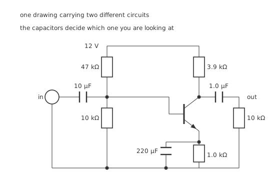
One drawing carrying two circuits, and the capacitors decide which one you are looking at.
The bias is the network the biasing lesson builds, unchanged and for the same reasons. What is added here is signal, and the three capacitors are how signal and bias are kept out of each other's way.
The input capacitor stops the source's DC from disturbing the base and stops the base's bias from being loaded by the source. The output capacitor does the same at the other end, so the load never sees the collector's several volts of standing DC. The bypass capacitor shorts the emitter resistor for signals while leaving it fully in place for DC, which is the trick that recovers all the gain the emitter resistor would otherwise cost.
Worked example — From the bias current to the gain
The bias network — 47 kΩ and 10 kΩ across 12 V, with 1.0 kΩ in the emitter, a junction drop of 0.70 V and a gain of 150 — sets 1.32 mA, which at 25.9 mV gives a transconductance of 51.2 mS.
The collector drives 3.9 kΩ and 10 kΩ in parallel, which is 2.81 kΩ.
Multiply and the gain is -144, or 43.1 dB. The minus sign is the inversion.
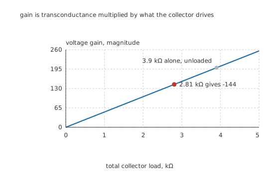
Gain is transconductance multiplied by what the collector actually drives.
Two things about that line are worth noticing. It goes through the origin, so the gain really is proportional to the load and there is no fixed part — a collector driving nothing has no gain at all. And the operating point sits well below where the collector resistor alone would put it, because the load has halved what the collector drives.
Engineer
What the stage offers at each end, and where the bottom end runs out
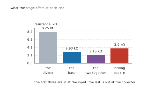
The divider is in parallel with the base, so the smaller of them wins.
Worked example — The input and output resistances
Looking into the base alone, the stage presents 2.93 kΩ — the gain divided by the transconductance.
But the divider is across it, and 8.25 kΩ in parallel with 2.93 kΩ gives 2.16 kΩ.
Looking back in at the collector, the transistor behaves as a current source and contributes almost nothing, so the output resistance is essentially 3.9 kΩ — the collector resistor.
That output resistance is the stage's real weakness. It is high enough that anything but a light load pulls the gain down, which is exactly what the 10 kΩ load did here. Driving a heavier load properly needs a follower after it.
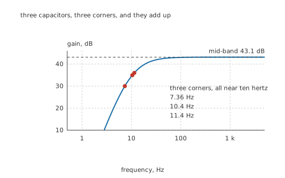
Three capacitors, three corners, and they add up.
Worked example — Where each capacitor gives up
The input capacitor 10 µF works against the stage's own 2.16 kΩ, giving 7.36 Hz.
The output capacitor 1.0 µF works against 3.9 kΩ and 10 kΩ in series, giving 11.4 Hz.
The bypass capacitor 220 µF has the hardest job. Looking into the emitter, the stage offers only 19.5 Ω, and that in parallel with the emitter resistor gives 69.3 Ω — which is why the bypass has to be the largest of the three to reach 10.4 Hz.
Putting three corners at the same frequency is a mistake that looks like tidiness. Each section is 3 dB down at its own corner, so three of them together are 9 dB down there rather than 3. Where the bottom of the passband matters, the usual practice is to put one corner at the wanted frequency and the other two a decade below it.
Professional
Swing, distortion, and the trade that connects them
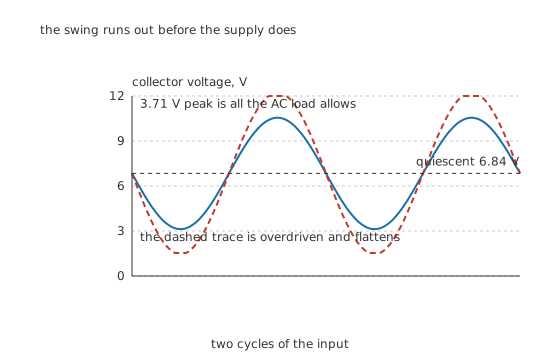
The swing runs out before the supply does.
Worked example — How far the output can actually go
The DC picture suggests plenty of room: the collector sits at 6.84 V with 5.51 V across the device, so 5.31 V of downward swing before it saturates.
The AC picture is tighter. For signals the collector drives 2.81 kΩ, not 3.9 kΩ, and the whole quiescent current has to be diverted to swing that far. That caps the peak at 3.71 V, which is the smaller number and therefore the real one. (The downward figure takes the device down to a saturation voltage of 0.20 V.)
The input that produces it is 25.9 mV — and that is not a coincidence. Divide the swing limit by the gain and the collector load cancels out completely, leaving exactly the thermal voltage. A bypassed common-emitter stage always runs out of clean swing at about twenty-six millivolts of input, whatever else is chosen.
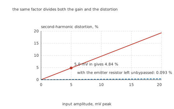
The same factor divides both the gain and the distortion.
Worked example — What the gain is actually costing
Drive the bypassed stage with 5.0 mV and the second harmonic comes out at 4.84 %, because the junction's exponential is being swung over a range comparable with 25.9 mV.
Remove the bypass capacitor. The gain collapses from -144 to -2.75, a factor of 52.2.
The distortion falls by the same 52.2, from 4.84 % to 0.093 %.
Those two factors are the same number because they are the same mechanism. The emitter resistor is negative feedback: it subtracts a copy of the output current from the input voltage, which reduces the gain and reduces the gain's dependence on anything, including on the signal itself. Nonlinearity is dependence on the signal, so it goes down by exactly the factor the gain does.
Four ways this stage is used in practice
Partly bypassed. Splitting the emitter resistor into a bypassed part and an unbypassed part sets the trade anywhere between the two extremes. It is the standard answer when neither end of the trade is acceptable.
As the first stage of a bigger amplifier. Its input resistance is moderate and its output resistance high, which is a bad match for a load but a fine match for another stage's base. Cascading is how discrete amplifiers reach useful gain.
With the collector resistor replaced by a current source. A mirror in place of the resistor gives a far higher AC load without costing DC headroom, and the gain rises accordingly. That is how integrated amplifiers do it and why they reach gains a resistor-loaded stage cannot.
Not for driving anything heavy. A loudspeaker, a relay or a long cable will pull this stage's gain down and clip it early. That job belongs to a follower or a push-pull output.
Two more limits worth knowing about
The top end has corners too. This lesson's three capacitors set the bottom of the response; the device's own capacitances and the Miller effect set the top. A common-emitter stage's high-frequency response is worse than the transistor's own, because the collector's inverted swing is fed back through the base-collector capacitance and multiplied by the gain.
Gain drifts with everything the bias drifts with. Transconductance is proportional to collector current, so the 7 % that temperature moves the bias by moves the gain by the same 7 %. Where gain has to be stable, feedback is the answer rather than a better bias network.
Common mistakes
- Calculating the gain from the collector resistor alone — the load is in parallel with it. Here 3.9 kΩ becomes 2.81 kΩ once the 10 kΩ load is connected, and the gain falls with it.
- Putting all three low-frequency corners at the wanted frequency — each is 3 dB down at its own corner, so three together are 9 dB down. Put one there and the others a decade lower.
- Undersizing the bypass capacitor — it works against 69.3 Ω here, not against the 1.0 kΩ emitter resistor, so it has to be the largest of the three by a wide margin.
- Expecting the DC headroom to be the available swing — 5.31 V of DC room becomes 3.71 V of usable peak once the AC load is taken into account, because signal current flows into the load as well as the collector resistor.
- Driving a bypassed stage hard for more output — at 5.0 mV in it is already producing 4.84 % second harmonic. The stage runs out of linearity long before it runs out of supply.
Parts used in this topic
Frequently asked questions
Why does a common-emitter stage invert?
Because the output is taken from a resistor between the collector and the supply. More base voltage means more collector current, more current means a bigger drop across that resistor, and a bigger drop means a lower collector voltage. Nothing was arranged to produce the inversion; the topology has no other option.
How is the voltage gain worked out?
Transconductance times the total load the collector drives. At 1.32 mA the transconductance is 51.2 mS, and 3.9 kΩ in parallel with a 10 kΩ load is 2.81 kΩ, giving a gain of -144 or 43.1 dB. It is proportional to the load with no fixed part, so a collector driving nothing has no gain.
What does the bypass capacitor actually do?
It shorts the emitter resistor for signals while leaving it in place for DC. That keeps the bias stability the emitter resistor provides and recovers the gain it would otherwise cost — here a factor of 52.2, from -2.75 up to -144.
How much input can the stage take before it distorts?
Less than you would expect. At 5.0 mV peak it already produces 4.84 % second harmonic, and the clean swing limit is 25.9 mV — exactly the thermal voltage, because the load cancels when you divide the swing limit by the gain. Leaving the emitter resistor unbypassed divides the distortion by 52.2 and the gain by the same factor.
Why is the usable swing smaller than the DC headroom?
Because signal current flows into the load as well as through the collector resistor. The device has 5.51 V across it and could in principle swing 5.31 V down, but the AC load of 2.81 kΩ means the quiescent 1.32 mA can only produce 3.71 V of swing before the collector current runs out.
Knowledge check
A stage biased at 1.32 mA has a 3.9 kΩ collector resistor and drives a 10 kΩ load. What is the gain? (Show answer)
What input resistance does the stage present, and why is it not simply the base's? (Show answer)
Where do the three low-frequency corners sit, and which capacitor has the hardest job? (Show answer)
How far can this stage's output swing cleanly, and what sets the limit? (Show answer)
What happens if the bypass capacitor is removed? (Show answer)
One email a month from the bench
New circuits, lessons, part guides and calculators, on the first Sunday of each month.