
A common-collector stage, or emitter follower, takes its output at the emitter: no voltage gain, but high input resistance and very low output resistance. A common-base stage drives the emitter and takes the output at the collector: full voltage gain, no current gain, and a much wider bandwidth.
Intuition
The interpreter who adds nothing but carries
Somebody speaking quietly at the front of a hall is perfectly clear to the people nearest them and inaudible at the back. An interpreter standing beside them who repeats every word at the same volume has added nothing — same words, same emphasis, no interpretation at all — and yet the room now works, because the interpreter has the lungs to fill it and the speaker does not.
An emitter follower is that interpreter. Its output voltage copies its input voltage almost exactly. It has no voltage gain and it does not pretend to. What it has is the ability to supply current, so a weak source can drive a heavy load through it without being pulled down.
The third arrangement goes the other way. Common base drives the emitter instead of the base, and takes the output at the collector. That gives the full voltage gain a common-emitter stage would, but no current gain at all — the current going in comes out again, barely diminished.
Three arrangements, three bargains. The common-emitter stage gets both voltage and current gain and pays with a limited bandwidth. The follower gives up voltage gain and gets an impedance transformation. The common-base stage gives up current gain and gets speed. There is no arrangement that wins twice, and knowing which one is being asked for is most of the skill.
Practitioner
Which terminal is left alone
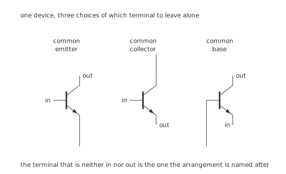
The terminal that is neither input nor output is the one the arrangement is named after.
The naming trips people up, so it is worth stating plainly. Each arrangement is named for the terminal that carries neither the input nor the output — the one tied to a rail and therefore common to both signal paths.
Worked example — One bias point, shared by all three
An 82 kΩ and 33 kΩ divider on 15 V with 2.2 kΩ in the emitter offers 4.30 V behind 23.5 kΩ. Taking off the junction's 0.70 V sets 1.52 mA and puts the emitter at 3.37 V.
At that current the transconductance is 58.8 mS, the emitter looks like 17.0 Ω from outside, and the base looks like 2.55 kΩ.
Those three numbers, plus the 150 current gain and the 0.9934 that follows from it, produce every figure in this lesson.
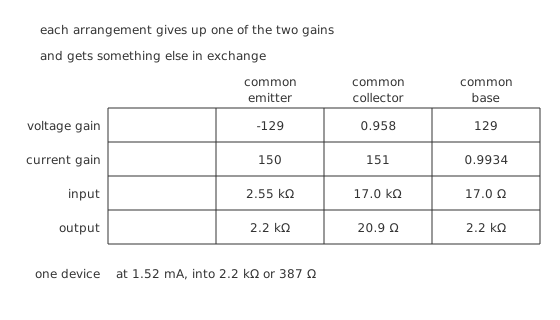
Each arrangement gives up one of the two gains and gets something else back.
Read that table by columns rather than rows. The common-emitter column is the only one with both gains in it. The follower's voltage gain is 0.958, which is not a gain at all — but look at what its input and output resistances are doing. The common-base column has the full voltage gain of 129, non-inverting this time, and a current gain of 0.9934, which is slightly less than one.
Engineer
What the follower is actually for
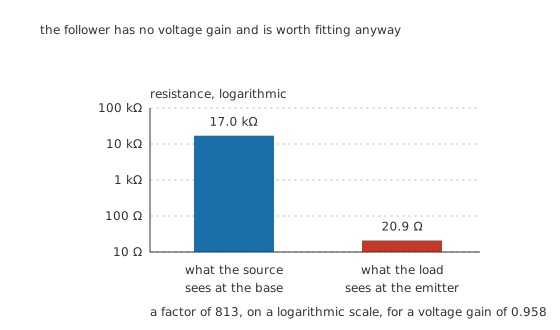
A factor of 813, bought for a voltage gain of less than one.
Worked example — The transformation, both ways
The emitter drives 2.2 kΩ and a 470 Ω load in parallel, which is 387 Ω. Nearly all of the input voltage lands on that rather than on the emitter's own 17.0 Ω, so the gain is 0.958.
Looking in at the base, the load appears multiplied by the gain plus one. 387 Ω becomes 61.0 kΩ at the base, and only the divider's 23.5 kΩ across it brings the stage's input down to 17.0 kΩ.
Looking back in at the emitter, the source's resistance appears divided by the same factor. A 600 Ω source becomes 20.9 Ω at the emitter.
That is a factor of 813 between the two ends, and it is the entire reason to fit the stage.
Notice which resistance the divider ruined. The base itself offers 61.0 kΩ, and the bias network throws most of that away. Where the high input resistance is the point, the divider has to be made much stiffer than bias stability alone would require, or bootstrapped so that it does not load the base at signal frequencies.
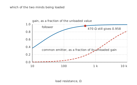
Only one of the two minds being loaded.
Worked example — Why the follower barely notices the load
The follower's gain is the load divided by the load plus 17.0 Ω. With 470 Ω in the picture, that is 0.958 — a loss of four per cent.
The common-emitter stage's gain, by contrast, is proportional to what its collector drives. A load equal to its own 2.2 kΩ halves it.
The follower only begins to sag when the load approaches 17.0 Ω, which is a couple of decades further down.
Professional
What the common-base arrangement is for
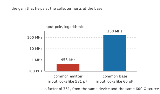
The gain that helps at the collector hurts at the base.
Worked example — The capacitance one arrangement multiplies and the other does not
A transistor's base-to-collector capacitance is small — 4.0 pF here. But in a common-emitter stage the collector swings -129 times as far as the base, and in the opposite direction, so the charge that capacitance demands is as if it were 4.0 pF multiplied by one plus the gain.
Add the base's own 60 pF and the input looks like 581 pF. Against a 600 Ω source that puts the pole at 456 kHz.
Drive the emitter instead. The base is now on a rail and does not swing, so nothing is multiplied. The input sees 60 pF against 16.5 Ω — the source in parallel with the emitter's own low resistance — and the pole lands at 160 MHz.
That is a factor of 351 from the same device at the same current, and it is why every wideband discrete stage is either common base or built from the arrangement below.
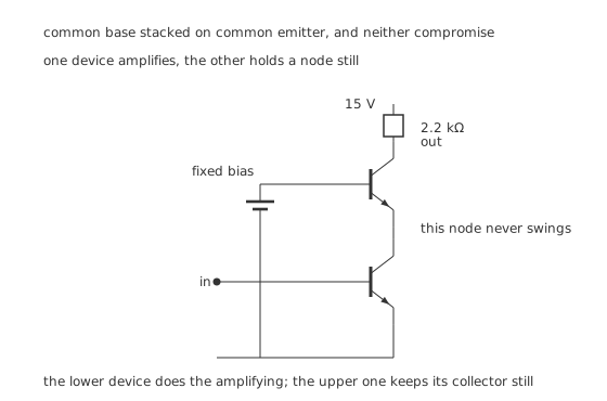
One device amplifies, the other holds a node still.
The cascode, and why it exists
Stack a common-base stage directly on top of a common-emitter stage and the compromise disappears. The lower device does the amplifying and keeps its high input resistance. Its collector, though, no longer swings — it is pinned by the upper device's emitter, which is held at whatever the upper base's fixed bias makes it.
With no swing at the lower collector, there is no multiplication of its base-to-collector capacitance, so the lower device keeps the common-base bandwidth. The signal current passes straight through the upper device and into the collector resistor, where all the voltage swing happens. The arrangement keeps the gain of one and the bandwidth of the other, at the cost of one more device and a couple of volts of headroom.
Where each one belongs
Follower at the output of anything. A common-emitter stage's 2.2 kΩ output resistance cannot drive a load without losing gain to it. A follower after it fixes that for the price of one transistor and a resistor. It is also the standard input stage where a source must not be loaded.
Follower as a rail buffer. The same low output resistance makes it a serviceable series pass element, which is exactly what it is doing inside a linear regulator.
Common base at radio frequencies, and as a current buffer. Its low input resistance is a good match for a transmission line, and its output current tracks its input current almost exactly.
Cascode wherever gain and bandwidth are both wanted. It is the standard high-frequency amplifier, and the same arrangement appears in the differential pair and in the input stages of most integrated amplifiers.
Three things that catch people out
A follower can oscillate. Its output resistance is low but slightly inductive at high frequency, and a capacitive load turns that into a resonant circuit with gain around it. A small resistor in series with the base — a few tens to a few hundred ohms — is the standard cure and costs almost nothing.
A follower's output cannot go below its own emitter voltage minus a junction drop. It follows the input downwards only until the transistor turns off, after which the emitter resistor alone has to discharge the load. For a heavy or capacitive load that asymmetry is severe, and the answer is a push-pull pair.
A common-base stage still needs its base properly grounded for signals. Any impedance in the base lead is multiplied by the same mechanism the arrangement was chosen to avoid, so a decoupling capacitor right at the base is not optional.
Common mistakes
- Expecting voltage gain from a follower — it is 0.958 here and can never exceed one. The stage is fitted for its 813-to-one impedance transformation, not for gain.
- Letting the bias divider spoil the follower's input resistance — the base alone offers 61.0 kΩ and the 23.5 kΩ divider drags the stage down to 17.0 kΩ. Where the high input matters, the divider has to be stiffer or bootstrapped.
- Naming the arrangement after the terminal the input arrives at — it is named after the terminal carrying neither input nor output, which is the one tied to a rail.
- Driving a capacitive load from a follower with no base resistor — the combination is a resonant circuit with gain around it, and a few tens of ohms in the base lead is the standard cure.
- Leaving a common-base stage's base decoupling to a distant capacitor — any impedance in that lead reintroduces the very multiplication the arrangement was chosen to avoid.
Frequently asked questions
If an emitter follower has no voltage gain, what is it for?
Impedance transformation. It presents 17.0 kΩ to whatever drives it and only 20.9 Ω to whatever it drives, a factor of 813. A weak source can therefore drive a heavy load through it without being pulled down, which is a job no amount of voltage gain would do.
Why does a common-base stage have so much more bandwidth?
Because its base does not swing, so nothing multiplies the base-to-collector capacitance. In common emitter that 4.0 pF looks like 581 pF at the input once the gain of -129 has multiplied it, putting the pole at 456 kHz. In common base the input sees only the 60 pF base capacitance and the pole is at 160 MHz — 351 times higher.
What is a cascode and why bother?
A common-emitter stage with a common-base stage stacked on top of it. The lower device's collector is pinned by the upper device's emitter, so it never swings and nothing is multiplied, while the signal current passes through to the collector resistor unchanged. It keeps the common-emitter gain and the common-base bandwidth for the price of one extra transistor.
How does the follower's input resistance get so high?
The load at the emitter appears at the base multiplied by the current gain plus one. Here 387 Ω at the emitter becomes 61.0 kΩ at the base. The bias divider's 23.5 kΩ then sits across that and brings the stage down to 17.0 kΩ, which is why the divider is often the limiting factor.
Which arrangement should I reach for first?
Common emitter, for gain. Add a follower when the load is too heavy for the collector resistor. Reach for common base or a cascode when the bandwidth of the common-emitter stage is the thing that has run out, which for this device and source happens at about 456 kHz.
Knowledge check
Name each arrangement's common terminal and say what it gives up. (Show answer)
An emitter follower drives 470 Ω through a 2.2 kΩ emitter resistor from a 600 Ω source. What does each end see? (Show answer)
Why is the common-emitter stage's bandwidth so much worse than the common-base stage's? (Show answer)
What does a cascode achieve that neither stage does alone? (Show answer)
Why does the follower barely lose gain into a load while the common-emitter stage does? (Show answer)
One email a month from the bench
New circuits, lessons, part guides and calculators, on the first Sunday of each month.