
Quick Answer
A bipolar junction transistor is a sandwich of three doped semiconductor layers, NPN or PNP, whose middle layer is made deliberately thin. Current injected into that middle layer controls a much larger current flowing straight through the sandwich, and the ratio between the two is the device's current gain.
Intuition
Most of the crowd walks straight past the till
Picture a shop with one narrow checkout area between the entrance and the stockroom. Customers pour in from the street, cross the checkout floor, and almost all of them keep going into the stockroom without stopping. Only a handful get caught at the till. If you widen the checkout floor, more people stop; make it narrow enough and the fraction who stop becomes tiny.
The number of people caught at the till is not impressive on its own. What is useful is that it tells you exactly how many went past — because the ratio is fixed by the geometry of the room, not by how busy the day is. Count the till receipts, multiply, and you know the traffic through the stockroom.
A bipolar junction transistor works on that arrangement, in silicon. It is three layers: a heavily doped emitter, a very thin and lightly doped base, and a collector. Charge injected out of the emitter has to cross the base to reach the collector, and because the base is thin, almost all of it does. A small fraction is caught in the base, and that fraction is the base current.
So the base current is small, the collector current is large, and the ratio between them is a property of the device rather than of the circuit. Feed the base a little and the collector will carry a lot. That is the whole idea, and everything else in this department is a consequence of it.
Practitioner
Three layers, and the middle one is deliberately thin
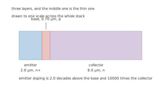
The base is the thinnest layer, and that is not an accident of manufacture.
Two things about that stack matter and neither is obvious from the symbol.
The base is thin — under a micron across, against several microns for the layers either side of it. And the emitter is doped far more heavily than the base, by 2.0 decades here, so when the emitter-base junction is forward biased the traffic across it runs overwhelmingly one way: out of the emitter, into the base. The collector, doped more lightly still, is there to collect.
Put those together and the device's behaviour follows. Charge leaves the emitter, enters the base, and has a very short distance to cross before the collector's field takes it. Only what recombines on the way stays behind as base current.
Worked example — One bias point, three currents
Drive the base from a 5.0 V logic level through 220 kΩ. The base-emitter junction holds about 0.70 V, so the resistor sees the rest and passes 19.5 µA.
With a current gain of 150, the collector carries 2.93 mA, and the emitter carries both of them together: 2.95 mA.
The base's share of that total is 0.662 %. Everything else went straight through.
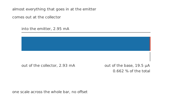
The base's share is drawn at the same scale as the collector's, which is why it is a sliver.
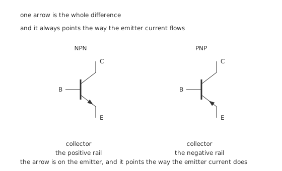
Both symbols, and the one difference between them.
NPN and PNP are the same device with every layer's doping swapped. The symbols differ by one thing: the direction of the arrow on the emitter, which always points the way the emitter's conventional current flows. On an NPN it points out of the device and the collector goes to the more positive rail. On a PNP it points in, and the collector goes to the more negative one. Get that backwards and nothing works, so it is worth reading the arrow every time rather than remembering which is which.
Engineer
Where the gain actually comes from
Current gain arrives in datasheets as a number, which makes it look like a property somebody chose. It is not. It is what falls out of the base's thickness.
Charge crossing the base is diffusing, and diffusing charge has a characteristic distance it travels before it recombines. Call that the diffusion length. If the base is much thinner than that distance, almost everything crosses; if it is comparable, a serious fraction is lost on the way. The fraction that survives is the base transport factor, and the gain is that fraction divided by what is left over.
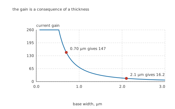
Three times the base width, a ninth of the gain.
Worked example — What a thicker base would cost
With a diffusion length of 6.0 µm, a base 0.70 µm across passes a fraction 0.9932 of what the emitter injects, which is a gain of 147.
Widen the base to 2.1 µm — 3.0 times as thick — and the fraction falls to 0.9417, a gain of 16.2.
That is 9.08 times less gain for three times the thickness, which is why base width is the dimension a process engineer fights hardest for.
The same arithmetic explains why the ratio between collector and emitter current is such an awkward number to think in. Nearly everything gets through, so that ratio sits at 0.9934 — close enough to one that quoting it to three figures tells you almost nothing, while the base ratio it implies is 150. Both describe the same device; only one of them has any resolution left in it. That is why base current, not emitter current, is the quantity every biasing calculation works from.
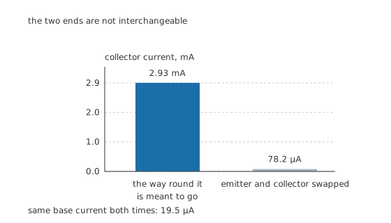
The two outer layers are not interchangeable, and the meter says so.
Worked example — Fitting one the wrong way round
Swap the emitter and collector leads and the device still conducts — it is still two junctions and one thin base. But the heavily doped layer is now doing the collecting rather than the injecting, and the injection efficiency that gave the gain has gone.
The same 19.5 µA now produces only 78.2 µA, on a reverse gain of 4.0.
The device is working 37.5 times worse than it should. It is a genuinely common wiring mistake, and it presents as a circuit that half works rather than one that is dead.
Professional
What the model leaves out, and what it costs you
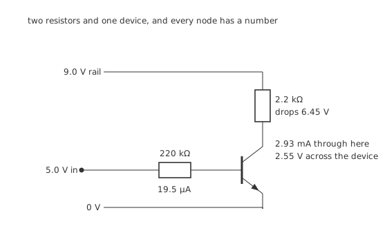
Every node in the circuit has a number, and every number came from one gain.
Worked example — What the device is dissipating
The collector current of 2.93 mA drops 6.45 V across 2.2 kΩ, leaving 2.55 V between collector and emitter on a 9.0 V rail.
The transistor is therefore dissipating 7.48 mW, which is what a small plastic package handles without comment.
That calculation used one number for the gain, and treating gain as a number is the first thing a real design has to stop doing.
Four things the datasheet will not let you assume
Gain is a range, not a value. Parts sold under one number routinely span a factor of three in gain, and the spread is a sorting decision at the factory rather than a defect. A circuit whose behaviour depends on the exact gain will work on one device and not on the next. Biasing exists almost entirely to remove that dependence, and the gain figure itself deserves its own reading.
Gain moves with current and with temperature. It peaks somewhere in the middle of the device's useful current range and falls off at both ends, and it climbs with temperature. None of that is visible in a single quoted figure.
The base-emitter drop is not 0.70 V. It is a junction like any other, so it follows an exponential and shifts with temperature by about two millivolts per degree. Using a fixed value is a working approximation for a bias calculation and a bad one for anything that has to hold still.
The collector is not a perfect current sink. Collector current creeps up as the collector-emitter voltage rises, because the depletion region eats into the base and effectively thins it. That is the Early effect, and the small-signal model is where it stops being a curiosity.
Two things the arrangement gives you for free
It is a current amplifier that can be used as almost anything. Wire the load in the collector and you get voltage gain; wire it in the emitter and you get a buffer; drive the base hard enough and you get a switch. The device did not change.
It is cheap, rugged and forgiving of drive. The base needs current rather than a precise voltage, and any source that can supply that current through a resistor will do. Where a MOSFET demands a gate voltage inside a defined window, a BJT will run from almost anything with a resistor in front of it.
Common mistakes
- Reading the arrow as pointing at the base — it is on the emitter lead, and it points the way the emitter's conventional current flows. Out of the device means NPN; into it means PNP.
- Swapping the emitter and collector leads — the device still conducts, so nothing looks obviously dead, but the gain collapses from 150 to 4.0 and the circuit half works.
- Treating the current gain as a constant of the part number — it varies by a factor of three between samples, and with current and temperature on top of that.
- Driving the base from a voltage source with no resistor — the base-emitter junction is a forward-biased diode, and a voltage source across it passes whatever current it takes to destroy the device.
- Assuming a PNP is upside down rather than mirrored — its collector goes to the more negative rail, but the base still needs to be driven towards the emitter to turn the device on, which for a PNP means pulled down.
Frequently asked questions
Why does a BJT need base current at all, when a MOSFET needs none?
Because the base-emitter junction is forward biased, and a forward-biased junction conducts. The base current is the fraction of the emitter's injected charge that recombines in the base instead of crossing it. A MOSFET's gate is insulated, so no equivalent path exists at all — which is the main practical difference between the two families.
What does the current gain of 150 actually mean here?
That the collector carries 150 times the base current, as long as the device has enough voltage across it to stay in its active region. Here 19.5 µA of base current gives 2.93 mA of collector current. It is not a promise: parts sold under one number span a wide range, and the figure moves with current and temperature.
Can I use a transistor with its emitter and collector swapped?
It will conduct, and that is the trap. The heavily doped layer is now collecting rather than injecting, so the gain falls to about 4.0 instead of 150 — the same 19.5 µA of base current gives 78.2 µA instead of 2.93 mA. The circuit half works, which is harder to diagnose than one that does not work at all.
Why is the base made so thin?
Because gain depends on it directly. With a 6.0 µm diffusion length, a 0.70 µm base gives a gain of 147; widening it to 2.1 µm drops that to 16.2. Charge crossing the base has to survive the trip, and a shorter trip means fewer losses.
Is NPN or PNP the one to reach for?
NPN, unless the circuit gives you a reason otherwise. Electrons move more easily than holes in silicon, so NPN parts are generally faster and available in more variants, and most reference circuits are drawn that way. PNP earns its place where the load has to sit on the ground side or where a positive rail has to be switched from above it.