
Quick Answer
A PN junction is the boundary where p-type and n-type silicon meet. Carriers diffuse across it, leave fixed charged atoms behind, and that charge builds a field that stops further diffusion. The result is a barrier that forward bias lowers and reverse bias raises, which is where every diode's behaviour begins.
Intuition
The tug of war that ends level
Two teams pull on a rope. Neither side moves. It would be easy to say nothing is happening, and it would be wrong: both teams are pulling as hard as they can, and the rope between them is stretched taut. Stalemate is what a large effort in each direction looks like from outside.
A PN junction holds that stalemate in a sliver of crystal. On one side of the boundary sits silicon doped so that its spare charge carriers are positive; on the other, silicon doped so that its spare carriers are negative. The moment the two are made as one crystal, carriers wander from where there are many of them to where there are few. That wandering is one team pulling.
But a carrier that wanders leaves something behind. The atom it came from is fixed in the crystal lattice and is now charged, because the mobile carrier that used to balance it has gone. Do that on both sides and you get a strip either side of the boundary with no mobile carriers in it at all, positively charged on one side and negatively charged on the other. That strip is called the depletion region, and the charge in it makes an electric field.
The field is the other team. It pushes carriers back exactly against the direction they were wandering, and it grows as more of them wander, so it eventually pushes back hard enough to stop the wandering altogether. The rope goes taut and stops moving.
What matters is that this happened without anybody connecting anything. The barrier is not something you apply to a junction, it is something the junction does to itself. Everything a diode is comes from that, and from one further fact: you can lean on the rope from outside. Push one way and the barrier gets smaller and carriers pour across. Pull the other way and the barrier gets bigger and the strip gets wider.
Practitioner
What the barrier is, and what leaning on it does
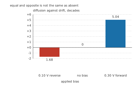
Equal and opposite is not the same as absent.
The two flows have names. Diffusion is carriers spreading out from where they are crowded, and it wants to push current across the boundary. Drift is the field sweeping the few carriers that stray into the depletion region back the way they came. At equilibrium these are the same size, so the net current is zero while both currents are still running.
The step in potential between the two sides is the built-in potential. For a silicon junction it lands somewhere near 0.70 V, the value this lesson works with throughout, and it is a property of the materials and the doping rather than something you can measure with a voltmeter across the diode's leads.
Diffusion is exponential in the barrier height, which gives the junction its most useful number. Every 59.5 mV that the barrier falls multiplies the diffusion current by ten.
Worked example — How far out of balance a small bias puts a junction
The thermal voltage at 300 K is 25.85 mV, and multiplying it by the natural logarithm of ten gives 59.5 mV per decade of current.
Lean on the junction by 0.30 V in the forward direction and the diffusion current climbs 5.04 decades above the drift current it used to match.
Lean the other way by 0.10 V and it falls 1.68 decades below it, so all that is left is the drift current, and that barely depends on the bias at all.
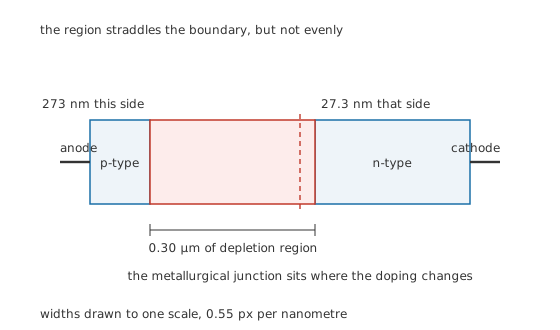
The region straddles the boundary, but not evenly.
The depletion region for the junction in this lesson is 0.30 µm wide with nothing connected, and it is not centred on the boundary. This junction's n side is doped 10 times more heavily, so the region reaches 273 nm into the p side and only 27.3 nm into the n side. The rule behind that is worth carrying: the depletion region spreads into whichever side is doped more lightly.
Engineer
Where the numbers come from
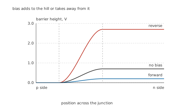
Bias adds to the hill or takes away from it.
Applied bias appears almost entirely across the depletion region, because that is the only part of the crystal without mobile carriers in it and therefore the only part with any real resistance. So the barrier a carrier has to climb is the built-in potential minus whatever forward bias you apply, or plus whatever reverse bias you apply.
That gives the two conditions the rest of this department is built on. Forward bias of 0.50 V leaves a barrier of 0.20 V, low enough that carriers cross it in numbers. Reverse bias of 2.0 V raises it to 2.70 V, and essentially nothing crosses.
Why the region is lopsided
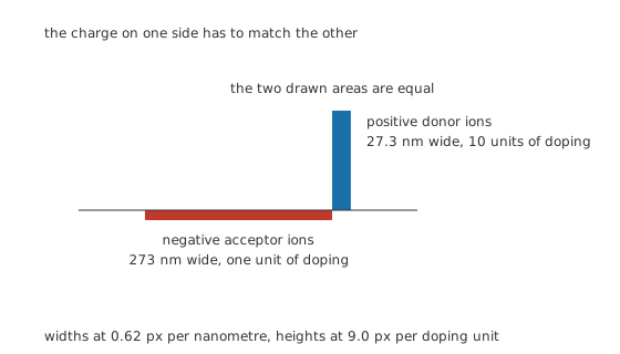
The charge on one side has to match the other.
The crystal as a whole is neutral, so the fixed positive charge uncovered on the n side must equal the fixed negative charge uncovered on the p side. Charge is doping density multiplied by width, so ten times the doping needs a tenth of the width. That single sentence explains the 273 nm against 27.3 nm split, and it explains why a diode designed to hold off a high reverse voltage has one very lightly doped side: the voltage has to be spread over distance, and only a lightly doped region gives it that distance.
How the width follows the voltage
Uncovering more charge takes more voltage, and the voltage needed grows faster than the width does, because each extra slice of uncovered charge sits further from the boundary and contributes more potential. The result is a square-root law: the width is proportional to the square root of the total potential across the region.
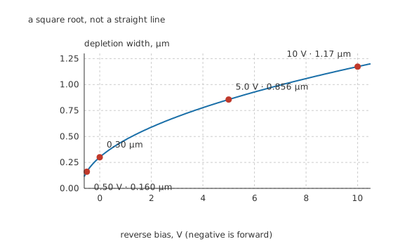
A square root, not a straight line.
At 0.50 V forward the region narrows to 0.160 µm. At 2.0 V reverse it is 0.589 µm, at 5.0 V it is 0.856 µm, and at 10 V it is 1.17 µm. Fifteen times the total potential gives just under four times the width.
The field inside the region is a triangle with its peak at the boundary, and the area under that triangle is the potential across the region. So the peak field is twice the potential divided by the width, which for the unbiased junction here is 4.67 MV/m. That number is the whole reason reverse breakdown exists: a few volts across a third of a micrometre is a field strong enough to tear carriers out of the lattice, and Zener diodes are built to do exactly that on purpose.
Professional
What the model leaves out, and what the junction costs you
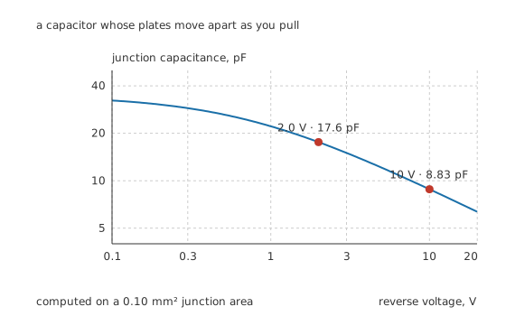
A capacitor whose plates move apart as you pull.
A region with no mobile carriers, sandwiched between two conductive regions, is a capacitor. Its dielectric is the silicon itself, at a relative permittivity of 11.7, and its plate spacing is the depletion width, which the bias sets. Working the parallel-plate calculation on a junction area of 0.10 mm² with a permittivity of free space of 8.854 pF/m gives 34.5 pF unbiased, 17.6 pF at 2.0 V and 8.83 pF at 10 V — a span of 3.91 times.
Both signs of that matter. A voltage-controlled capacitance is a useful thing, and tuned circuits are built on it. It is also the reason a reverse-biased junction cannot switch off instantly: turning it off means charging a capacitor whose value changes as you do it, and Schottky diodes exist partly because they avoid a related storage effect entirely.
The three simplifications this lesson made
The doping was treated as changing abruptly at the boundary. Real junctions are graded, because dopants diffuse during manufacture. A graded junction still widens with reverse voltage, but the exponent is nearer one third than one half, so the capacitance curve above is the right shape for the wrong process. The idea survives, the exact numbers do not.
The bias was assumed to appear entirely across the depletion region. At high forward currents the neutral regions either side stop being negligible and add a genuine series resistance, so the barrier stops falling as fast as the applied voltage suggests. That is why the exponential model in diode I-V characteristics bends over at the top.
The temperature was fixed at 300 K. Two separate things move with it. The thermal voltage rises in direct proportion to absolute temperature, which stretches the exponential out. Working against that, the number of carriers generated thermally rises very much faster, which is what pulls the built-in potential down and makes the reverse leakage of a silicon junction roughly double for every ten degrees. The second effect wins, and the practical consequence is that a junction's forward voltage falls as it warms up while its reverse leakage climbs.
Where the leakage actually comes from
The drift current in the equilibrium picture is small because the carriers it sweeps are the ones thermally generated inside or near the depletion region. That makes reverse leakage a generation rate rather than a conduction, and it explains two things that otherwise look odd. Leakage barely depends on reverse voltage, because generation does not care how hard the field pulls once the carriers are being collected. And it depends enormously on temperature and on the volume of the depletion region, which is why a physically large, high-voltage rectifier leaks more than a small signal diode of the same material.
Sensing that generation deliberately, instead of tolerating it, is what a photodiode does.
Common mistakes
- Thinking equilibrium means nothing is flowing — diffusion and drift are both running at full size and cancelling. That is why a small bias produces such a large change so quickly.
- Expecting to measure the built-in potential with a voltmeter — the contacts to the semiconductor form their own junctions whose potentials cancel it exactly, so an unbiased diode reads zero.
- Assuming the depletion region sits symmetrically on the boundary — it spreads into whichever side is doped more lightly, in inverse proportion to the doping.
- Treating the depletion width as proportional to reverse voltage — it follows a square root, so ten volts widens it by about four times rather than ten.
- Ignoring junction capacitance in a reverse-biased circuit — it is a real capacitance of tens of picofarads on an ordinary rectifier, it varies with the voltage across it, and it is what limits switching speed.
Frequently asked questions
What is a PN junction?
It is the boundary inside one crystal where p-type material meets n-type material. Mobile carriers diffuse across it and leave fixed charged atoms behind, which creates an internal electric field that opposes further diffusion. The region emptied of mobile carriers is the depletion region, and the potential step across it is the built-in potential.
Why does a diode conduct one way and not the other?
Because bias adds to or subtracts from the barrier the diffusion current has to climb, and that current depends exponentially on barrier height. Forward bias lowers the barrier and the current rises very steeply. Reverse bias raises it, leaving only the small drift current, which comes from thermal generation and hardly changes with voltage.
Why can I not measure the built-in potential across a diode?
Because measuring it means attaching metal to both semiconductor regions, and each of those metal-to-semiconductor contacts has a potential step of its own. Going right around the loop, the contact potentials cancel the junction's exactly. A junction with nothing applied has no net voltage around any closed path, which is what stops it being a battery.
What is the depletion region?
It is the strip either side of the boundary that mobile carriers have left, so all that remains there is the fixed charge of the dopant atoms. It behaves as an insulator between two conductive regions, and its width changes with the applied bias: narrower under forward bias, wider under reverse bias.
Why does reverse leakage double for every ten degrees?
Reverse current is set by how fast carriers are thermally generated in and around the depletion region, not by how hard the field pulls on them. Generation rate climbs very steeply with temperature, so leakage climbs with it. The exact factor varies with the material and the mechanism, and roughly a doubling per ten degrees is the working rule for silicon.