
Quick Answer
An insulated-gate bipolar transistor drives a bipolar output stage from a MOSFET's insulated gate. It conducts with a fixed voltage drop rather than a resistance, which wins at high current and high voltage, and it turns off slowly because stored charge has to recombine first.
Intuition
A light touch on the handle of a heavy machine
A crane operator moves several tonnes with a joystick. The joystick takes no effort at all — it is not connected to the load in any mechanical sense — and everything heavy happens somewhere else, in response to it.
An IGBT is that arrangement in one package. A small insulated-gate device does the listening, and its output becomes the drive for a large bipolar device that does the work. The gate takes no steady current, exactly as a MOSFET's does not; the thing being controlled conducts like a bipolar transistor, with a voltage drop that hardly changes with current.
That combination is worth having for one reason and costs you for another.
Worth having: a fixed drop of a volt or two beats a resistance once the current is large. A MOSFET's loss grows as the square of its current, and there is a current above which no MOSFET of a given voltage rating can compete.
The cost: the bipolar half fills its drift region with charge to conduct that well, and turning the gate off does not remove it. The charge has to recombine, which takes microseconds, during which the device is still passing current with the full bus across it. That tail is the reason IGBTs do not go fast.
So the family occupies a defined corner: high voltage, high current, moderate frequency. Below that corner a MOSFET is better. Above it in frequency a MOSFET is better again. The whole of this lesson is working out where the boundaries actually fall.
Safety
Devices in this class are used on mains-derived buses, in motor drives, inverters and induction heaters. The illustrative 600 V bus worked through here is high enough to be lethal, and a bus like it stays live after disconnection because the capacitors that support it hold their charge. Assume any such bus is live until you have measured it. Nothing in this lesson is a substitute for the working practice in electrical safety, and no number here is drawn from any standard — the bus voltage, both devices' parameters and every edge time are illustrations chosen to make the arithmetic concrete.
Practitioner
What is actually inside
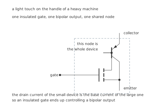
One insulated gate, one bipolar output, one shared node.
The equivalent circuit is two devices and one internal node, and that node is the whole idea. The small device's drain current is the large device's base current. Nothing else is connected there.
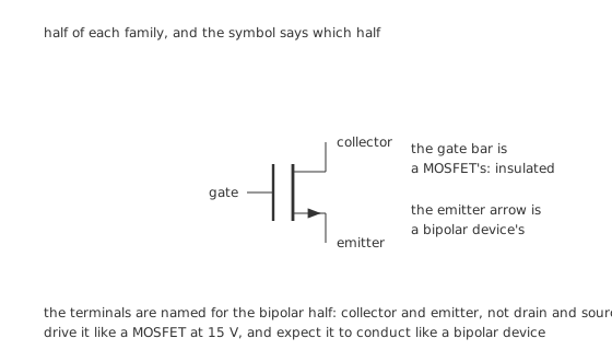
Half of each family, and the symbol says which half.
The symbol borrows from both parents and so do the terminal names. It has a gate, driven like a MOSFET's and typically to 15 V. It has a collector and an emitter rather than a drain and a source, which is the standing reminder that the conducting half is bipolar.
Worked example — Conduction loss, both ways round
Take an illustrative device holding 1.8 V when on, against a MOSFET of the same voltage rating holding 190 mΩ.
At 50 A the IGBT loses 90.0 W and the MOSFET loses 475 W — a factor of 5.28.
At 5.0 A the answer reverses: 9.00 W for the IGBT against 4.75 W for the MOSFET, a factor of 1.89 the other way.
Engineer
The two crossings that decide which device to use
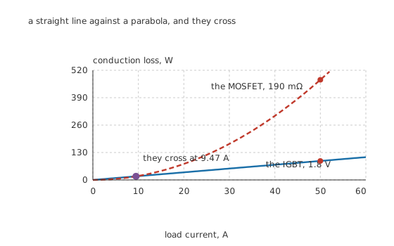
A straight line against a parabola, and they cross once.
Worked example — Where the current crossover falls
A fixed drop gives a loss proportional to current; a resistance gives one proportional to its square. Setting them equal, the crossover is simply the saturation voltage divided by the on-resistance.
Here that is 9.47 A.
Below it the MOSFET wins and above it the IGBT does, and because one curve is a parabola the gap widens quickly in both directions. That single number, not the datasheet's headline figures, is what a designer is really comparing.
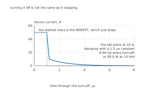
Turning it off is not the same as it stopping.
Worked example — What the edges and the tail cost
Switching 50 A on a 600 V bus at 10 kHz, with edges of 100 ns and 200 ns, costs the IGBT 45.0 W. The MOSFET's faster 40 ns and 30 ns cost it 10.5 W.
Then the tail. The IGBT's current falls quickly to 10 A — 0.20 of the load — and decays from there with a 1.5 µs time constant, against the full bus.
That is 9.00 mJ at every turn-off, or 90.0 W at 10 kHz. The tail alone costs more than the edges and the conduction put together, which is the fact most people meet only after building something.
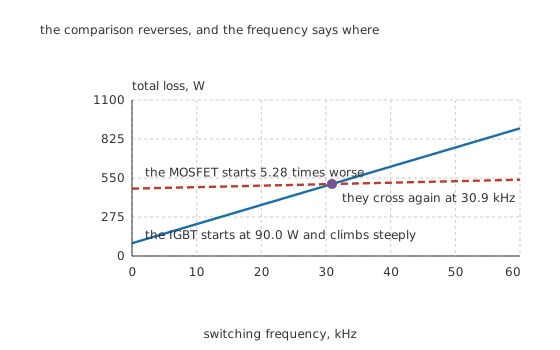
The comparison reverses, and the frequency says where.
Worked example — The second crossing, in frequency
Add everything up at 10 kHz. The IGBT loses 225 W and the MOSFET 486 W, so at this current and this frequency the IGBT is comfortably ahead.
But the IGBT's total climbs steeply with frequency and the MOSFET's barely moves. They cross again at 30.9 kHz.
Above that frequency the MOSFET is the better device even at 50 A, despite starting 5.28 times worse on conduction alone. Neither the current crossover nor the frequency crossover decides on its own; the operating point has to be checked against both.
Professional
What has to be added, and what has to be avoided
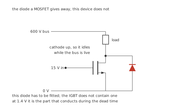
The diode a MOSFET gives away, this device does not.
Worked example — The component the structure does not include
A MOSFET's body region gives it a built-in diode from source to drain whether anyone wanted one or not. An IGBT's structure does not produce one, so a bridge built from IGBTs has no freewheel path unless a diode is fitted.
Cathode to the collector, anode to the emitter. While the bus holds the collector positive it is reverse biased and idle; when an inductive load drags the collector down at turn-off it conducts at about 1.4 V and carries the current.
Many IGBTs are sold in a package that already contains this diode, and many are not. Which one you have is a datasheet question with a hardware consequence, and leaving the diode out of an inductive bridge destroys the devices on the first turn-off.
Four things that decide whether an IGBT design works
Check both crossings, not one. The current crossover here is 9.47 A and the frequency crossover 30.9 kHz. A design at high current and low frequency is squarely IGBT territory; one at high current and high frequency may not be, and the arithmetic is the only way to know.
Drive the gate properly. It is a MOSFET gate with a MOSFET gate's capacitance, and a slow edge means the device spends longer in the region where it is dissipating heavily. Everything in gate drive applies unchanged, and the consequences are larger because the bus is larger.
Respect the dead time. In a bridge, both devices of a leg conducting at once puts the bus across two devices in series with nothing to limit the current. The IGBT's tail makes that harder to avoid than it is with MOSFETs, because the device is still conducting after its gate has gone. The H-bridge lesson treats the failure in full.
Watch for latch-up. The equivalent circuit has a second, parasitic bipolar device in it that the real structure cannot avoid. Under a large enough current transient the pair can latch into conduction and stop responding to the gate at all, which is destructive. Modern devices are designed to make it very unlikely; it is a bounded region on the datasheet rather than an impossibility.
Where the family sits now
Silicon carbide MOSFETs have taken the top of the frequency range. They hold off high voltages without the drift-region penalty that makes a silicon MOSFET impractical there, so they occupy exactly the corner where an IGBT's tail was the limiting factor. IGBTs remain dominant where the current is very large and the frequency modest.
The applications have not changed. Motor drives, solar inverters, uninterruptible supplies, induction heating and traction are all high-current, high-voltage, moderate-frequency work. That corner is exactly where the two crossings computed above put the device.
Common mistakes
- Choosing on conduction loss alone — at 50 A the IGBT is 5.28 times better, and at 30.9 kHz that advantage has been eaten entirely by the tail and the slower edges.
- Assuming a body diode exists — an IGBT's structure does not produce one. An inductive bridge without a fitted diode destroys its devices on the first turn-off.
- Forgetting the tail in the thermal budget — 9.00 mJ per turn-off is 90.0 W at 10 kHz, more than the conduction loss and the edge loss added together.
- Using one below its current crossover — under 9.47 A here a MOSFET of the same rating loses less, and at 5.0 A it loses 1.89 times less.
- Setting dead time as if the gate controlled the current — the device conducts after its gate has gone, so the dead time has to cover the tail rather than only the edge.
Frequently asked questions
What is an IGBT actually made of?
A small insulated-gate device whose drain current feeds the base of a large bipolar device, in one structure. Those two things are the only ones on the internal node, which is why an insulated gate that takes no current ends up controlling a bipolar output that conducts with a fixed voltage drop.
When is an IGBT better than a MOSFET?
Above the current where a fixed drop beats a resistance — 9.47 A for the pair compared here — and below the frequency where the IGBT's slower edges and its tail catch up, which is 30.9 kHz at 50 A. High current, high voltage and moderate frequency is the corner.
What is the tail current and why does it matter so much?
When the gate turns off, the charge that made the on-state voltage low is still in the drift region and has to recombine. Here the current falls quickly to 10 A and then decays with a 1.5 µs constant, against the full 600 V bus. That is 9.00 mJ per turn-off, or 90.0 W at 10 kHz — more than the conduction and edge losses together.
Does an IGBT have a body diode like a MOSFET?
No. The structure does not produce one, so a freewheel diode has to be fitted across it — cathode to the collector — in any inductive application. Some parts are sold in a package that already contains one, and the datasheet is the only way to tell.
How should the gate be driven?
Like a MOSFET's, typically to 15 V, and through a driver capable of moving the gate charge quickly. The gate takes no steady current but it is a capacitor, and a slow edge means longer spent in the region where the device dissipates heavily — which on a 600 V bus is expensive.