
Quick Answer
A junction field-effect transistor conducts through a channel whose width is squeezed by the depletion region of a reverse-biased gate junction. It passes full current with no gate drive and turns off as the gate goes negative, drawing almost no gate current in the process.
Intuition
Narrowing the channel without touching it
Look at a river running through a gorge: what throttles it is the rock either side, not anything in the water. Push the walls closer and less gets through; push them until they meet and nothing does. The walls never touch the water and take nothing from it.
A JFET works that way. Its channel is a bar of doped silicon with the drain at one end and the source at the other, and current runs along it as it would along a resistor. Beside the channel sits a gate of the opposite doping type, and the junction between them is held reverse biased — which is the point, because a reverse-biased junction has a depletion region, and that depletion region reaches into the channel and narrows it.
Make the gate more negative and the depletion region grows, the channel narrows, and less current flows. Make it negative enough and the depletion regions from both sides meet, and the channel is closed.
Two consequences follow, and they are the reasons anyone reaches for the part. The gate takes essentially no current, because it is a reverse-biased junction rather than a forward-biased one. And the device is on by default — with the gate doing nothing, the channel is wide open. A bipolar transistor is off until driven; a JFET is on until driven.
Practitioner
The channel, and what closes it
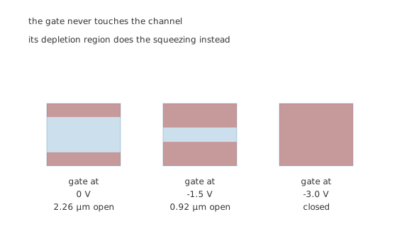
The gate never touches the channel; its depletion region does the squeezing.
Worked example — The geometry, and what it lets through
With the gate at zero volts the junction still has its own built-in 0.70 V across it, so the depletion region already reaches 0.87 µm into a half-channel of 2.0 µm. That leaves 2.26 µm open, and the device passes its full 10 mA.
Take the gate to -1.5 V and the depletion region reaches 1.54 µm, leaving only 0.92 µm open. The current falls to 2.50 mA.
At -3.0 V the two depletion regions meet and the channel is closed. That voltage is the device's pinch-off, and it is set by the doping and the channel thickness rather than chosen.
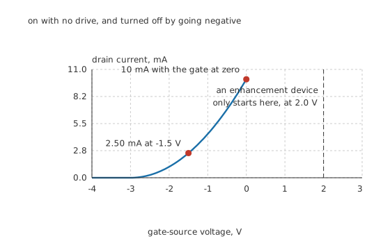
The two families of field-effect device do not overlap at all.
The whole of a JFET's useful range is at negative gate voltages — for an n-channel part, at least, and the p-channel version is the mirror image. That is the single biggest practical difference from an enhancement MOSFET, whose threshold sits on the other side of zero — 2.0 V for the device drawn beside it — and which conducts nothing at all until driven past that. Nothing about a circuit designed for one will work with the other in its place.
Engineer
What the quiet gate costs, and what it is worth
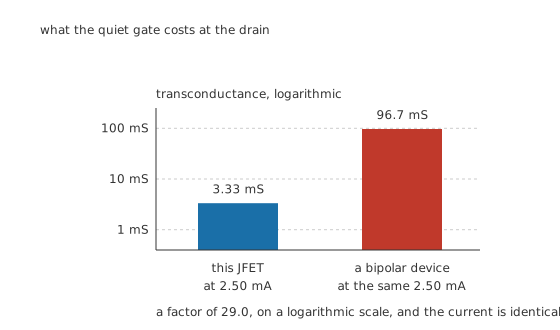
A factor of 29, at identical current.
Worked example — The gain the square law gives up
The square law's slope at zero gate is twice the zero-gate current divided by the pinch-off voltage, or 6.67 mS. At the operating point that has fallen to 3.33 mS.
A bipolar device at the same 2.50 mA would offer 96.7 mS, because its current follows an exponential rather than a square law.
That is 29.0 times more transconductance from the same current, and it is the price a JFET stage pays. A single JFET stage's voltage gain is correspondingly modest.
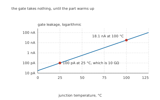
The gate takes nothing, until the part warms up.
Worked example — What the gate is actually worth
At 25 °C the gate leaks 100 pA, so a 1.0 V source driving it sees 10 GΩ. Nothing a bipolar base could approach.
The catch is that a reverse-biased junction's leakage roughly doubles every 10 °C. At 100 °C the same gate leaks 18.1 nA, and the source now sees 55.2 MΩ.
A fall of 181 for seventy-five degrees. Still an excellent input, but a design that depends on gigohms at room temperature has nothing left at the top of its range.
That trade is the whole selection argument. A JFET is chosen where a source must not be loaded — high-impedance probes, electrometers, condenser microphones, the front end of an instrument. It is not chosen for gain, and a stage that needs both usually puts a JFET at the input and something else after it.
Professional
Biasing a part whose spread is enormous
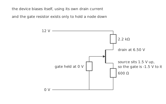
The device biases itself, using its own drain current.
Self-bias is the arrangement almost every discrete JFET circuit uses, and it is neat: the drain current lifts the source above ground, the gate is held at ground by a resistor that carries nothing, so the gate ends up negative with respect to the source by exactly the amount that current produces.
Worked example — Sizing the source resistor
Pick the operating point first: 2.50 mA at -1.5 V.
The source resistor has to drop that voltage at that current, so it is 600 Ω.
On a 12 V rail through 2.2 kΩ the drain lands at 6.50 V, which leaves room to swing.
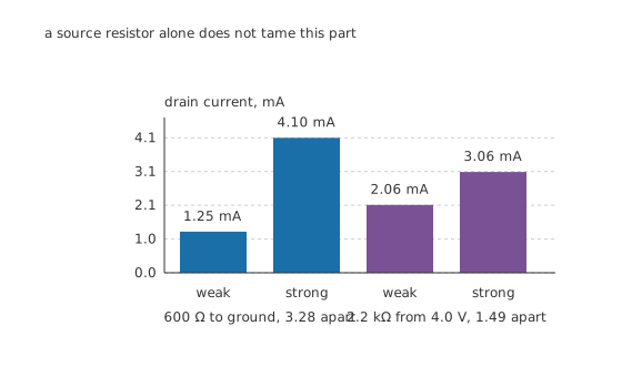
A source resistor alone does not tame this part.
Worked example — What that arrangement does about the spread — which is less than it looks
Parts sold under one number span an enormous range: 5.0 mA to 20 mA of zero-gate current, a factor of 4.0, with pinch-off anywhere from -1.5 V to -4.5 V.
Run the two extremes through the 600 Ω self-bias and they land at 1.25 mA and 4.10 mA — still 3.28 apart. The scheme has barely touched it.
Lift the gate to 4.0 V from a divider and put 2.2 kΩ in the source instead, so the source has to sit much higher to reach the same gate-source voltage. Now the extremes give 2.06 mA and 3.06 mA, only 1.49 apart.
The improvement is bought entirely with supply voltage. The larger source resistor drops several volts that the drain circuit no longer has, which is why JFET stages tend to want a higher rail than an equivalent bipolar one.
Four things about the part that are easy to get wrong
The gate must never be driven positive far. It is a junction, and forward biasing it turns the device into a diode drawing whatever current the source will supply. A series resistor in the gate lead costs nothing and prevents the whole class of accident.
The drain and source are often interchangeable. In a symmetrical part they are, physically — which is convenient until it is not, because the datasheet parameters are quoted for one orientation and a reversed part may measure differently.
Below pinch-off the device is a resistor, not a current source. With the drain only a fraction of a volt above the source, the channel behaves ohmically and its resistance is controlled by the gate. That region is a nuisance in an amplifier and the whole point in a voltage-controlled attenuator or an analogue switch.
Nothing about this part is precise. With a four-to-one spread in zero-gate current and a three-to-one spread in pinch-off, any circuit that needs a defined drain current needs either a stiff bias arrangement, individual adjustment, or a topology that does not care — which is why JFETs so often appear as followers and as current sources rather than as gain stages.
Where the family goes from here
The JFET is the older of the two field-effect families and the less common one now. Its successor, the MOSFET, replaces the reverse-biased junction with an actual insulator, which removes the leakage problem entirely and allows the gate to be driven positive. What the MOSFET keeps is the idea this lesson is about: a channel whose conductance is set by a field rather than by an injected current.
Where the JFET survives is at the input of low-noise, high-impedance amplifiers, where its lack of gate current and its comparatively benign noise behaviour still beat a bipolar input, and in the constant-current arrangement where its self-biasing simplicity is worth more than its accuracy is worth worrying about.
Common mistakes
- Expecting it to be off with no gate drive — a JFET passes its full 10 mA with the gate at zero. It is a depletion device, and something has to turn it off.
- Driving the gate positive — the gate is a junction, not an insulator, and forward biasing it turns the part into a diode across the input.
- Designing for a defined drain current from a source resistor alone — a four-to-one part spread still leaves 3.28 to one after plain self-bias, from 1.25 mA to 4.10 mA.
- Assuming the gate stays a gigohm — 100 pA at 25 °C becomes 18.1 nA at 100 °C, so 10 GΩ falls to 55.2 MΩ. Leakage doubles roughly every 10 °C.
- Expecting bipolar gain — at 2.50 mA a JFET offers 3.33 mS of transconductance against a bipolar device's 96.7 mS, a factor of 29. The quiet gate is paid for at the drain.
Frequently asked questions
Why is a JFET on when nothing is connected to its gate?
Because its channel is a continuous bar of doped silicon. Nothing has to be created to make it conduct; the gate's job is to narrow it. With the gate at zero the depletion region already reaches 0.87 µm into a 2.0 µm half-channel, but 2.26 µm is still open and the device passes its full 10 mA.
How much current does the gate take?
At room temperature, 100 pA for this part — an input resistance of 10 GΩ at 1.0 V. But that is a reverse-biased junction's leakage, which doubles about every 10 °C, so at 100 °C it has grown to 18.1 nA and the input has fallen to 55.2 MΩ.
Why do JFET amplifiers have so much less gain than bipolar ones?
Because the drain current follows a square law rather than an exponential, so the slope is far gentler. At 2.50 mA this part offers 3.33 mS against a bipolar device's 96.7 mS at the same current, a factor of 29, and gain is transconductance times load.
How does self-bias produce a negative gate voltage from a positive supply?
The drain current flows through the source resistor and lifts the source above ground. The gate is tied to ground through a resistor that carries no current, so it stays at ground — which means it is negative with respect to the source by exactly the source resistor's drop. Here 600 Ω at 2.50 mA gives the −1.5 V the device needs.
Is self-bias enough to handle the part spread?
Not on its own. A four-to-one spread in zero-gate current still leaves a 3.28 to one spread in drain current, from 1.25 mA to 4.10 mA. Lifting the gate to 4.0 V and using 2.2 kΩ in the source narrows it to 1.49 to one, but the extra source voltage comes out of the drain circuit's headroom.