
Quick Answer
Choosing the decoupling capacitor is the easy half and it is nearly always done correctly. The half that decides whether the board works is where the part physically sits, how much area the current's loop encloses on its way there and back, and what the vias and the return plane do to that loop.
Intuition
The loop, not the value
A town with one reservoir on a hill can still run out of water at a tap, and the reason is never the reservoir. It is the pipe. The water tower exists precisely because a main from a distant reservoir cannot answer a sudden demand fast enough, and a tower two streets away answers in seconds what the reservoir cannot answer in minutes.
Nobody sizes a water tower by asking how much water is in it. They ask how far it is from the tap.
Which capacitor to fit is a real question and that lesson answers it: the value, the family, the parallel combination, and the frequency at which two good capacitors are worse than one. This lesson assumes all of that has been decided correctly, which on most boards it has been, and asks the question that actually goes wrong afterwards.
Where does the part go, and what does the current have to travel through to get from it to the pin?
An invented chip carries the answer: a 1.8 V part with 4 supply pins and 32 outputs, each driving 12 pF, switching at 25 MHz with 800 ps edges, decoupled by 47 nF parts. Every number attached to it and to its board is an invention.
Practitioner
What the pin asks for, and how quickly
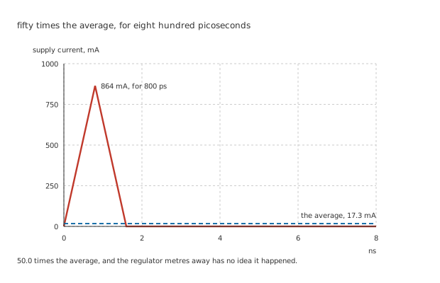
Fifty times the average, and the regulator metres away has no idea it happened.
The current a chip draws is not one number. It is a small average with enormous, brief spikes on it, and the two are answered by completely different things.
Worked example — The average, and then the peak
Every output that switches moves its load between the rails, so 32 of them at 25 MHz take 31.1 mW — an average of 17.3 mA from the 1.8 V rail.
But the charge does not arrive smoothly. Each transition moves 691 pC and it moves it in 800 ps, which is 864 mA.
That is 50.0 times the average, and a slew of 1.08 GA/s.
The regulator supplies the average and knows nothing about the peak: it is metres of track away and could not respond in 800 ps if it wanted to. The peak comes from whatever is close enough, which is the capacitor, and the only question left is how hard the trip is.
Engineer
The trip, and what makes it expensive
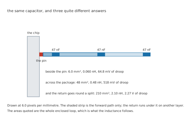
The shaded strip is the forward path only. The return runs under it on another layer.
Current going out and coming back encloses an area, and that area is an inductance. It is not a parasitic in the sense of something that crept in: it is the unavoidable consequence of the loop having a size, and it is the single number that decides whether the capacitor helps.
Worked example — What the geometry costs
An invented board gives 0.010 nH/mm² of loop inductance per square millimetre enclosed.
A capacitor beside the pin encloses 6.0 mm², or 0.060 nH, and 864 mA arriving in 800 ps through that demands 64.8 mV.
The same capacitor across the package encloses 48 mm², which is 0.48 nH and 518 mV — 8.00 times worse for a part that has not changed at all.
Two holes nobody drew on the schematic
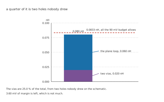
A quarter of the total, from two holes that appear on no schematic.
The plane loop is not the whole story, because the capacitor is on one side of the board and the planes are inside it.
Worked example — Adding the vias
2 vias at an invented 0.010 nH each add 0.020 nH, which is 25.0 % of the 0.080 nH the loop then has.
That gives 86.4 mV of droop, against a board noise budget of 90 mV.
Which leaves 3.60 mV of margin. It fits, and not by much.
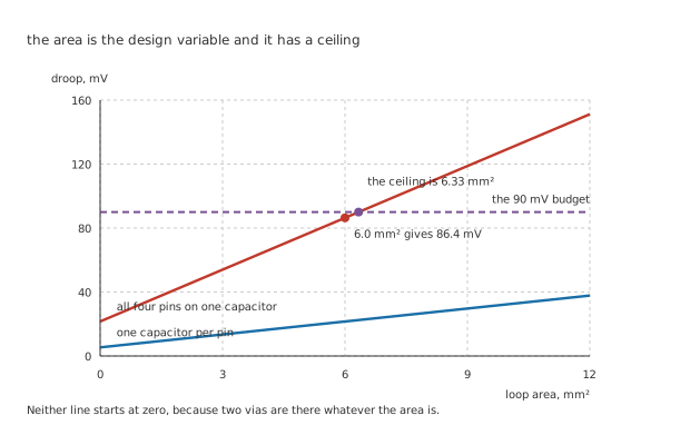
Neither line starts at zero, because two vias are there whatever the area is.
That budget of 90 mV is a board number the designer sets, not a family threshold. What the receiving parts will tolerate is a separate calculation and it sets what this budget is allowed to be.
Turned round, the budget puts a ceiling on the geometry: 0.0833 nH of total inductance, of which the vias have already taken 0.020 nH, leaving 6.33 mm² of loop area. The near placement at 6.0 mm² has 0.33 mm² of headroom, which is why "as close as you can" is a real instruction and not a slogan.
Professional
Four pins, and the plane underneath
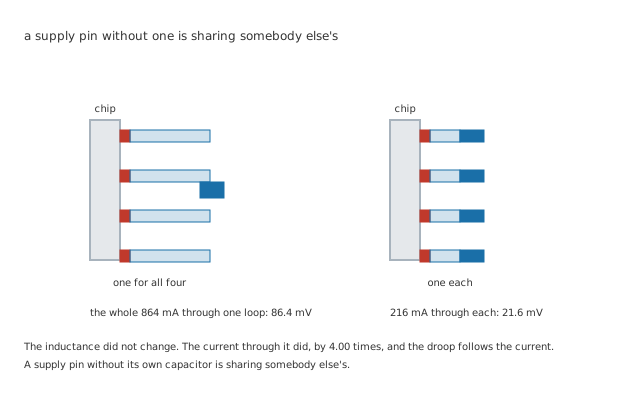
The inductance did not change. The current through it did.
Worked example — Why one good capacitor is not enough
With one capacitor serving all 4 pins, the whole 864 mA passes through a single 0.080 nH loop: 86.4 mV.
Give each pin its own and each loop carries 216 mA through the same inductance: 21.6 mV.
That is 4.00 times better without improving the layout by a single millimetre, because the droop follows the current and the current has been divided.
A supply pin without its own capacitor is sharing somebody else's, and it is sharing it through whatever path connects the two pins — which on a real package is longer than either capacitor's own loop.
The return current is half the loop and gets none of the attention
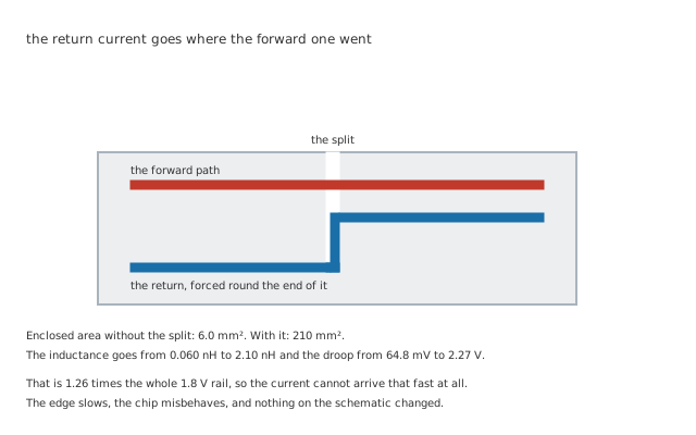
The enclosed area goes from 6.0 mm² to 210 mm², and nothing on the schematic changed.
At these speeds return current does not spread out and take the shortest path. It follows the forward path as closely as the copper allows, directly underneath it, because that is the arrangement with the least inductance and current at speed goes where the inductance is least.
Which means a plane is not a magic ground: it is a return conductor whose shape matters, and anything that interrupts it interrupts the return.
Worked example — What a slot costs
Cut a slot in the plane between the capacitor and the pin — for a connector, a row of vias, a deliberate split — and the return cannot cross it. It goes back to the slot, round the end, and forward again.
210 mm² of enclosed area is 2.10 nH, and the same current through it demands 2.27 V — 35.0 times the near placement's droop.
That is 1.26 times the whole 1.8 V rail, which is more voltage than exists. So the current does not arrive that fast at all: the edge slows, and the chip does something nobody asked it to.
That last step is worth being clear about, because the arithmetic looks like nonsense otherwise. The inductance does not produce a voltage larger than the supply. It refuses to let the current change that quickly, the edge stretches, and what the designer sees is a part that misses timing or resets intermittently on a board whose schematic is perfect.
Doing it, in order
Find the supply pins first, all of them. Then put one capacitor next to each, on the same side of the board as the chip if the layout allows it.
Keep the loop small in both directions. Short is good; short and directly over an unbroken return is what actually matters, and the two are not the same instruction.
Give the capacitor its own vias, and put them at the pads. 25.0 % of the loop was two holes here. Sharing vias with something else, or running a short track to a via somewhere convenient, adds more than the distance suggests.
Then look at the plane before you look at anything else. A slot, a row of through-hole pins, a plane split for an unrelated reason: any of them can turn a 6.0 mm² loop into a 210 mm² one without changing a component.
And check the bulk capacitor is somewhere too. The local part answers the edge; something larger answers the millisecond, and that division of labour is the other lesson's subject.
Common mistakes
- Choosing the value carefully and placing the part carelessly — 47 nF beside the pin gives 64.8 mV of droop and the same part across the package gives 518 mV, which is 8.00 times worse for an identical component.
- Sizing from the average current — the average is 17.3 mA and the peak is 864 mA, 50.0 times more, arriving in 800 ps. The capacitor exists for the second number.
- Ignoring the vias — two of them at 0.010 nH contribute 0.020 nH, which is 25.0 % of the 0.080 nH total and leaves only 3.60 mV of a 90 mV budget.
- One capacitor for several supply pins — the whole 864 mA then goes through one loop for 86.4 mV, against 21.6 mV when each pin has its own. The inductance was identical; the current was not.
- Treating the ground plane as a node rather than a conductor — return current follows the forward path underneath it, and a slot in the way turns 6.0 mm² of loop into 210 mm².
- Reading a droop larger than the rail as an arithmetic error — 2.27 V on a 1.8 V rail means the current cannot arrive that fast, so the edge stretches instead. That is the failure, and it looks like a timing fault rather than a supply one.
Frequently asked questions
Does the capacitor's own inductance matter as much as the loop's?
It matters, and on a small modern part it is usually the smaller of the two. A 0402 or 0201 ceramic's internal inductance is a fraction of what a millimetre of loop contributes, which is why the package got small long before anyone ran out of capacitance. The interesting consequence is that fitting a physically larger capacitor of the same value can make things worse.
Should the capacitor go on the same side as the chip, or underneath it?
Whichever gives the smaller loop, and that depends on the board. On a thin board with the planes close to the surface, directly underneath the pin on the far side can be excellent, because the vias are short and the loop is almost vertical. On a thick board the vias dominate and the same-side placement wins. It is worth working out rather than following a rule.
How close is close enough?
Here the budget answers it: 90 mV of droop allows 0.0833 nH, the vias take 0.020 nH, and 6.33 mm² of loop area is what remains. That is a specific number from a specific budget, and doing the same sum for your own board is the point of this lesson. The habitual answer of "a few millimetres" is a summary of that calculation done on typical boards, not a substitute for it.
Why does the return current follow the forward path instead of spreading out?
Because at these speeds inductance decides the path rather than resistance. At DC the return spreads to whatever offers the least resistance, which is the widest route. Above a few hundred kilohertz the least-inductance path wins instead, and that is the one directly under the forward conductor, where the two currents' magnetic fields cancel most completely.
Can I fix a bad layout with a bigger capacitor?
Almost never, and the arithmetic says why. The droop here is the inductance times the rate of change of current, and the capacitance does not appear in it at all. A larger capacitor holds more charge for the millisecond problem and does nothing whatever for the 800 ps one. The only fixes are a smaller loop, more loops in parallel, or a slower edge.