
Quick Answer
A digital input does not read a voltage, it reads which side of a threshold the voltage is on. Every family publishes four numbers: two the driver promises and two the receiver demands. The driver always promises more than the receiver asks for, and the gaps between them are how much noise the connection will survive.
Intuition
The gap is the whole point
A traffic light has three states and no others. It is never eleven per cent green. Whatever the bulb is doing electrically, the answer a driver takes from it is one of a very small set, and that is what makes a junction workable: nobody has to interpret.
Amber is the interesting one. It is not a fourth state so much as an admission that the light has to pass through something on its way between two useful ones, and the rule about amber is written precisely because the transition exists and someone has to be told what to do during it.
A digital signal works the same way and has the same amber. It is a real voltage on a real wire, wandering with noise and supply sag, and the receiving chip does not measure it. It compares it against a threshold and reports a side. Above one line it is a one; below another it is a zero; and between them is a region where the part is entitled to report anything at all.
Turning a continuum into a decision is that other lesson's subject. This one is about where the lines are, how much room there is between what a driver will produce and what a receiver will accept, and what happens when the two ends of a wire were designed against different lines.
Every number in this lesson is invented. Threshold voltages of this class belong to standards, and no standard's value is published here. Three made-up families carry the argument. The 3.3 V one drives above 2.90 V and below 0.35 V, and accepts above 2.30 V and below 0.95 V; the 1.8 V one drives above 1.55 V and below 0.25 V, accepting above 1.25 V and below 0.55 V; and the 5.0 V one is walked through in full below.
Practitioner
Four numbers, and the two gaps they leave
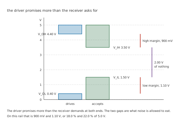
The gaps between the columns are the margins. Between the receiver's two demands lies 2.00 V in which nothing is defined.
The four numbers come in two pairs and it is worth being precise about who owes what to whom.
The driver's promise. 4.40 V is the lowest voltage it will produce for a one; 0.40 V is the highest it will produce for a zero. Both are worst-case commitments, made at the rated load current.
The receiver's demand. 3.50 V is the lowest voltage it will certainly read as a one; 1.50 V is the highest it will certainly read as a zero.
Worked example — Where the room comes from
The driver produces at least 4.40 V and the receiver needs only 3.50 V, so there is 900 mV of slack at the top.
At the bottom the driver produces at most 0.40 V and the receiver will accept up to 1.50 V, which is 1.10 V of slack.
Those are 18.0 % and 22.0 % of the 5.0 V rail, and they are the entire budget for everything that goes wrong on the wire.
Between 1.50 V and 3.50 V is 2.00 V of nothing. A receiver presented with a voltage in there has made no promise about what it will report, and the useful way to read that is not "it will guess" but "it may report either, and it may report both in quick succession".
Engineer
What the margin has to survive, and how it shrinks
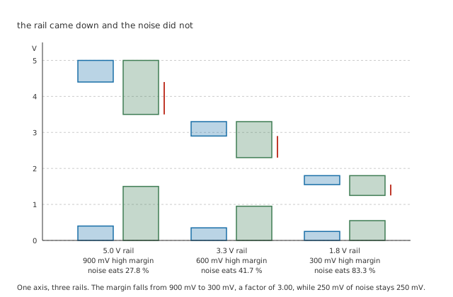
One axis, three rails, so the margins are comparable in millivolts rather than as percentages.
Every rail generation has cut the supply voltage, for good reasons that have nothing to do with noise: less dynamic power, thinner oxides, smaller transistors. The margins came down with it.
Worked example — A fixed disturbance against a shrinking budget
A 250 mV disturbance on the wire — a nearby edge, a ground bounce, a supply glitch — does not care what rail the family runs on.
Against the 5.0 V family's 900 mV it is 27.8 % of the margin. Against the 3.3 V family's 600 mV it is 41.7 %.
Against the 1.8 V family's 300 mV it is 83.3 %, and the margin has fallen by a factor of 3.00 while the disturbance has not moved at all.
The two lower families are symmetrical where the top one is not: 600 mV and 300 mV match their high margins exactly.
As a fraction of the rail the three families are similar — 18.0 %, 18.2 % and 16.7 % — which is exactly what makes the percentage the misleading way to look at it. Noise arrives in millivolts, not in per cent.
The edge is where the trouble starts
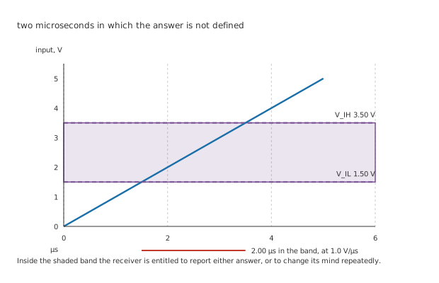
Inside the shaded band the receiver is entitled to report either answer, or to change its mind repeatedly.
A margin is a statement about a signal that has settled. During a transition the signal is by definition somewhere in between, and how long it spends there is a design number.
Worked example — How long the crossing takes
An edge rising at an invented 1.0 V/µs has to cross 2.00 V of undefined region.
That takes 2.00 µs, during which the receiver's output is not specified.
Hold the receiver to a 500 ns ceiling instead and the edge has to arrive at 4.00 V/µs, which is 4.00 times faster.
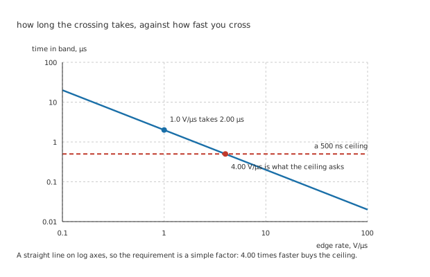
A straight line on log axes, so the requirement is a simple factor.
This is why "slow edges are fine, it is only DC" is one of the reliable ways to build something that works on the bench and fails in the field. A slow edge is a long invitation for noise to arrive while the answer is undefined, and the receiver's response to that is not a wrong answer but an unspecified one.
Professional
Two rails on one wire
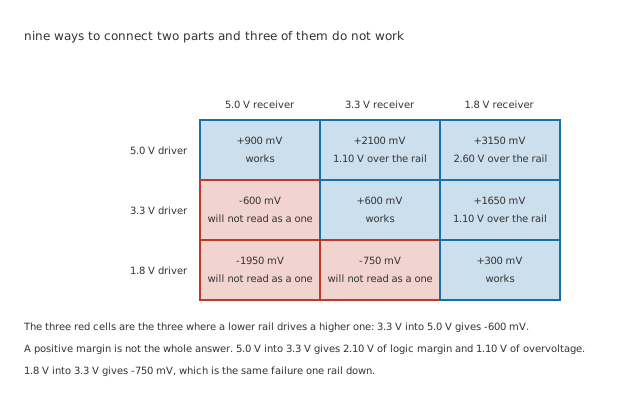
The diagonal is always positive because a family is specified against itself.
Nothing in the four numbers says both ends of a wire have to be the same family. Boards routinely mix rails, and the arithmetic is the same subtraction done across the boundary.
Worked example — Three that fail and three that need watching
A 3.3 V driver produces at least 2.90 V, and a 5.0 V receiver demands 3.50 V. The margin is -600 mV: negative, so a one may not read as a one.
A 1.8 V driver into a 3.3 V receiver gives -750 mV, the same failure one rail down.
Go the other way and a 5.0 V driver into a 3.3 V receiver has 2.10 V of logic margin — and presents 1.10 V more than the receiver's own rail, which is a different problem with the same cause.
Those two failures need different fixes and get confused constantly. Driving upward needs the signal raised, by a level shifter or a part with a lower threshold. Driving downward needs the signal limited, by a divider, a series resistor into a clamp, or a receiver specified as tolerant of more than its own rail.
Hysteresis, and where it actually sits
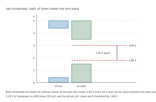
Both thresholds lie strictly inside the ordinary band, so the part is still an ordinary member of its family.
An input with hysteresis has two thresholds instead of one: it switches up at 3.00 V and back down at 1.80 V, 1.20 V apart. Once it has decided, the signal has to come a definite distance back before it will change its mind.
Worked example — What that buys on a slow edge
The 1.20 V of hysteresis is 4.80 times the 250 mV of noise, so noise alone cannot walk the input back across.
Both thresholds sit inside the family's own 2.00 V, so the part still satisfies 3.50 V and 1.50 V and can be used anywhere the plain one can.
The driver clears the upper threshold by 1.40 V and the lower one by 1.40 V.
What that positive feedback is doing inside is a circuit question that lesson answers. From outside it is simply two lines instead of one, and the practical rule is that any input fed by something slow, long or noisy wants a hysteretic one.
Reading a logic interface
Find the four numbers for both parts, not one. The margin is a subtraction across the boundary, and half the numbers belong to each end.
Check both directions. A bidirectional line is two interfaces and they can fail independently.
Then check the rails against each other, because a positive logic margin and an overvoltage are not mutually exclusive. 2.10 V of margin with 1.10 V of overvoltage is a working link that destroys the receiver.
And find out what an unconnected input does. An input left floating on a modern part is not at zero and is not at the rail: it sits wherever leakage and nearby signals leave it, drifting through the undefined band, and the output does whatever that implies. Every unused input needs tying somewhere deliberately, through a resistor or directly, and it is the single most common omission on a first board.
Common mistakes
- Reading the margin as a percentage — 18.0 %, 18.2 % and 16.7 % across three rails look interchangeable, and the actual budgets are 900 mV, 600 mV and 300 mV. Noise arrives in millivolts.
- Assuming a 3.3 V output drives a 5 V input — it gives a margin of -600 mV against a 3.50 V threshold, so a one is not guaranteed to read as a one. It often works, which is worse than failing.
- Assuming a 5 V output is safe into a 3.3 V input because the margin is large — 2.10 V of logic margin comes with 1.10 V above the receiver's own rail, and the second number is what breaks the part.
- Ignoring edge rate on a long or noisy line — at 1.0 V/µs an edge sits in the 2.00 V undefined band for 2.00 µs. Meeting a 500 ns ceiling needs 4.00 V/µs, four times faster.
- Leaving unused inputs unconnected — a floating input drifts through the undefined band and the output follows it, drawing current and oscillating. It is not pulled anywhere by default.
- Treating a Schmitt input as a different family — its 3.00 V and 1.80 V thresholds both sit inside the ordinary 1.50 V to 3.50 V band, so it meets the same specification and can go anywhere the plain part can.
Frequently asked questions
Why are the driver's numbers worst case rather than typical?
Because a promise that holds typically is not a promise. V_OH is specified at a stated output current, at the worst supply and temperature in the part's range, and a real part on a good day will do considerably better. Designing against the typical figure means designing against a number the manufacturer never agreed to, which works until the batch changes.
What actually happens if an input sits in the undefined band?
Two things, and the second is the expensive one. The output is unspecified, which may mean either level or a burst of transitions as noise moves the input back and forth across the internal threshold. Less obviously, on a CMOS input both halves of the first stage conduct at once, so the part draws real current from its supply — milliamps rather than the nanoamps it normally takes — and a chip full of floating inputs gets warm.
Is a series resistor enough to drive a 3.3 V input from a 5 V output?
On its own, no — a resistor limits current, not voltage, and with nothing to limit against the input still sees close to 5 V. It works when the receiver has clamp diodes to its own rail and the resistor keeps the current into them within what the datasheet allows, which is a real and widely used technique that has to be checked rather than assumed. A divider or a proper level shifter makes no such assumption.
Do the four numbers change with supply voltage and temperature?
Yes, which is why they are quoted with conditions attached. Thresholds on most modern families track the supply, so a part run at the bottom of its supply range has different absolute thresholds from the same part at the top. Where two parts share a signal and not a supply, that is one more thing the margin subtraction has to be done against.
Why not simply make the margins bigger?
Because they are the leftovers of decisions made for other reasons. The driver's V_OH is limited by its output stage's drop at the rated current, and the receiver's V_IH by where the input stage's threshold can be held over supply and temperature. Widening either costs something else — drive current, speed, process margin — and the numbers you see are where those trades landed.