
Quick Answer
A decoupling capacitor supplies the current a chip demands faster than the regulator can. At the speeds that matter, what limits it is the inductance of the loop between the capacitor and the pin, not the capacitance, so placement and the number of parallel paths decide the result.
Intuition
A torch beside the mains lamp
A room lit from the mains goes dark when the supply blinks, because the power station is a long way away and the wiring between takes time to respond. A torch on the table does not care: its energy is already in the room, centimetres from where it is needed.
Decoupling is that torch. A digital chip switching its outputs demands a burst of current in a few nanoseconds, and the regulator that feeds it is centimetres away down a track. Centimetres is a long way at those speeds. A capacitor beside the chip holds a local reserve of charge that arrives immediately, and the regulator refills it at its own pace afterwards.
That is the standard explanation, it is correct, and it leads almost everybody to the wrong conclusion. If the job is holding charge, more capacitance must be better, and a bigger capacitor must beat a smaller one. Both are false on a real board, and the reason is that the charge was never the difficulty.
The difficulty is getting the charge out. Between the capacitor's plates and the chip's pin there is a loop of copper, and a loop of copper is an inductance. Over a nanosecond-scale edge that inductance develops a voltage far larger than anything the capacitance was going to save. Everything practical about decoupling follows from that one fact.
Practitioner
Sizing it twice, and only one answer mattering
Take a chip on a 3.3 V rail that demands 2.0 A in 5.0 ns, with a budget of 100 mV of droop.
Worked example — Two sums, two different answers
Sized for charge alone: supplying 2.0 A for 5.0 ns within 100 mV takes 100 nF. That is where the ubiquitous hundred-nanofarad decoupling capacitor comes from, and it is a small, ordinary part.
Now the loop. With 2.0 nH between the capacitor and the pin, the same 2.0 A arriving in the same 5.0 ns develops 800 mV across that inductance. The budget was 100 mV, so the rail is over by a factor of 8.0.
The capacitance was correct and the design still fails. Nothing about choosing a larger capacitor changes the second sum.
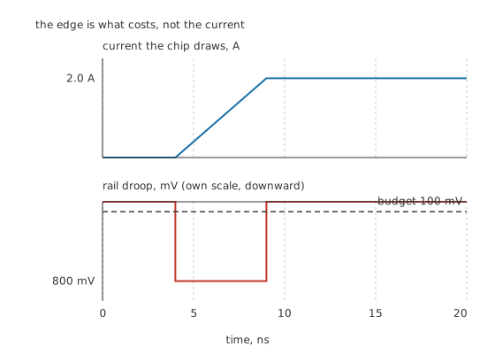
The edge is what costs, not the current.
What does change it is more paths. Put 8 capacitors in parallel, each with its own loop, and the inductances are in parallel too: 250 pH, and the droop falls to 100 mV, which meets the budget exactly. The series resistances divide by the same factor, from 30 mΩ to 3.75 mΩ.
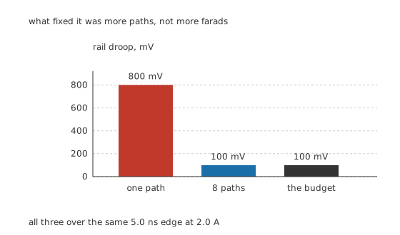
What fixed it was more paths, not more farads.
Eight small capacitors beat one capacitor eighty times larger, and the reason has nothing to do with charge. This is the single most consequential idea in board-level power design, and it is why decoupling advice is always about placement and count rather than value.
Engineer
The loop, and what actually sets its size
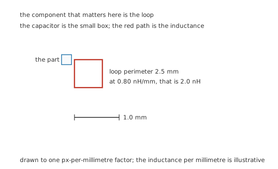
The capacitor is the small box. The red path is the inductance.
The inductance in that sum is not the capacitor's own. A modern chip capacitor contributes a fraction of a nanohenry; the rest is the loop the current traces: out of one terminal, along a track, through a via, across the plane, up another via, into the pin, and back. At an illustrative 0.80 nH/mm, a loop with a 2.5 millimetre perimeter comes to 2.0 nH.
Three things follow, and they are the whole of decoupling layout.
Distance is the enemy, in both directions. Both the outward path and the return path count. A capacitor placed beautifully close to a pin but returning its current the long way round has the same inductance as one placed badly.
Vias matter as much as tracks. A via has inductance comparable to a millimetre or two of track, so the number of vias in the loop is part of the answer. Two vias per capacitor terminal instead of one halves that contribution, and it costs board area rather than money.
Plane spacing sets the floor. Once the loop has been shortened as far as geometry allows, what remains is set by how far apart the power and ground planes are. Bringing them closer reduces the loop area for every capacitor on the board at once, which is why the stack-up is a decoupling decision rather than a mechanical one.
What paralleling does, and what it does not
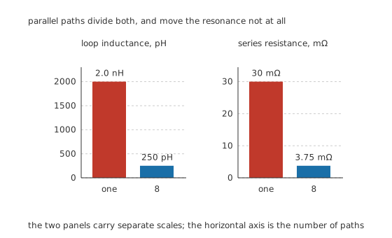
Parallel paths divide both, and move the resonance not at all.
Eight paths divide the inductance by eight and the resistance by eight. What they do not do is move the self-resonant frequency: the capacitance rises by the same factor the inductance falls, so the resonance stays where it was, at 11.25 MHz against 11.25 MHz for one part.
That is a useful thing to know because it kills a common misconception. Paralleling identical capacitors lowers the impedance floor and does nothing at all about where the parts stop being capacitors. To move that frequency you need a physically smaller package, not more of the same one.
Professional
The frequency where two good capacitors are worse than one
Real boards carry a bulk capacitor as well: a 10 µF part with 2.5 nH and 20 mΩ, to cover the slower demands the local parts cannot. Each part is a V curve with its own minimum, and the two minima are in different places: 1.007 MHz for the bulk part and 11.25 MHz for the local ones.
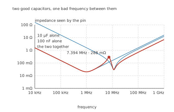
Two good capacitors, one bad frequency between them.
Between those two frequencies something unwelcome happens. The bulk part is already above its resonance and therefore inductive; the local part is still below its own and therefore capacitive. An inductance in parallel with a capacitance is a parallel resonant circuit, and at 7.394 MHz the pair reaches 288 mΩ: higher than either part alone would be at that frequency.
This is anti-resonance, and it is why "add a bulk capacitor and a small one" is a rule with a hole in it. The peak is real, it lands squarely in the range a fast digital board actually uses, and it is invisible to anybody who checks only that both capacitors are present and correct.
Three ways of dealing with it, in increasing order of effort.
Damp it. The peak's height is set by the losses in the two branches, so a part with more series resistance flattens it. That is why a deliberately lossy bulk capacitor sometimes outperforms a better one, and it is the one place in this department where higher ESR is the desirable property.
Fill the gap. More values between the two, so no single frequency has one branch inductive and the other capacitive by a wide margin. This is the origin of the decade-spaced capacitor sets that appear on reference designs.
Reduce the difference. Less inductance everywhere squeezes the range in which the mismatch exists. The layout work from Layer 3 helps here too.
Which store answers when
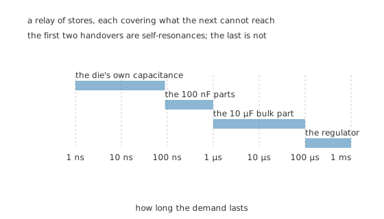
A relay of stores, each covering what the next cannot reach. The first two handovers are the self-resonances, not choices; the last, to the regulator, is not a resonance at all.
The mental model that survives contact with a real board is a relay rather than a reservoir. The die's own on-chip capacitance answers the first nanosecond because nothing on the board can. The local parts answer the next stretch. The bulk part answers beyond their resonance. The regulator answers everything slower than that. Each store covers the band the next one cannot reach, and the boundaries are set by physics rather than by preference.
Two selection consequences. First, the local parts want a low resonance-limited impedance rather than a large value, which means the smallest package with the lowest inductance rather than the highest capacitance. Second, a class 2 ceramic that delivers a fraction of its marked value under bias is often perfectly acceptable here, because the value was never the binding constraint. That is the opposite of the advice coupling capacitors needs, and the difference is exactly that one position cares about the value and the other cares about the impedance. Choosing the right capacitor sets the two side by side, and noise covers what the decoupling is protecting the rest of the board from.
Common mistakes
- Choosing a bigger capacitor when the rail droops — at nanosecond edges the droop comes from loop inductance, and capacitance does not enter into it. More parallel paths help; more farads on one path do not.
- Placing the capacitor near the pin but returning its current the long way — both halves of the loop count, and a good outward path with a bad return is a bad loop.
- Assuming paralleling moves the self-resonance — it lowers the impedance floor and leaves the resonant frequency exactly where it was, because capacitance and inductance change by the same factor.
- Fitting a bulk part and a small one and stopping there — between their two resonances one is inductive and the other capacitive, and the pair rings at a frequency where the combination is worse than either alone.
- Rejecting a class 2 ceramic here because of bias loss — in this position the impedance matters and the value does not, so a part delivering a fraction of its marking can still be the right choice.
Frequently asked questions
Why 100 nF? Where does that value come from?
From the charge sum: supplying a couple of amps for a few nanoseconds within a hundred millivolts of droop needs about that much. It is a real calculation with a real answer, and it is also the less important of the two sums, because the loop inductance usually dominates at those speeds.
Is one large capacitor as good as several small ones?
No, and usually much worse. Several capacitors give several parallel current paths, so the loop inductance divides by their number, and it is that inductance which limits how fast charge can arrive. One large part has one path however many farads it holds.
How close does a decoupling capacitor need to be?
Close enough that the whole current loop, outward path and return, is short. The distance to the pin is only half of it: a capacitor a millimetre from the pin whose return current travels ten millimetres has a ten-millimetre loop. Via count and plane spacing matter as much as the placement.
What is anti-resonance and why does it matter?
Between the self-resonances of two different capacitors, the larger one is already inductive while the smaller one is still capacitive. An inductance in parallel with a capacitance resonates, and at that frequency the pair presents a higher impedance than either part alone. It lands in the range fast digital boards actually use.
Does the dielectric matter for decoupling?
Less than anywhere else. The value is not the binding constraint here, so a class 2 ceramic that loses most of its marking under bias is often still the right part, because what is wanted is a low impedance in a very small package. What does matter is the package size, because that is what sets the inductance.