
Quick Answer
Ceramic capacitors come in two classes that behave nothing alike. Class 1, marked C0G, holds its value across temperature, bias and time. Class 2, marked X5R, X7R or Y5V, buys far more capacitance per package and gives back a large fraction of it under working voltage, heat and age.
Intuition
A sponge that stiffens as you squeeze it
Press a dry kitchen sponge and the first centimetre is easy. Press further and it fights back harder for each millimetre, because there is less air left to remove. The sponge has not been damaged and it will spring straight back; it simply gives less for each newton once it is already compressed.
A class 2 ceramic capacitor does the same thing with voltage. The dielectric is a material whose molecules line up with the field, and each one that has already lined up cannot line up again. Apply a working voltage and much of the material is already committed, so an extra volt moves far less charge than the first volt did. Measured as capacitance, the part is worth a fraction of its marked value while it is doing its job, and it recovers completely the moment the voltage comes off.
This is not a fault, not an ageing effect and not a bad batch. It is what the material is, and it is the single most surprising thing about the most common capacitor in the world.
Class 1 ceramics are a different material with a different mechanism, and they do none of it. They hold their value to a fraction of a percent across temperature and give up nothing at all to bias. What they give up is capacitance per package: for the same case size, a class 1 part offers two or three decades less. The two are sold under one word and they are not substitutes.
Practitioner
What the three characters promise, and what they leave out
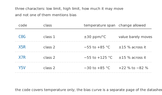
The code covers temperature only. The bias curve is a different page of the datasheet.
The code is three characters and each one means something. The first gives the lowest temperature the part is specified at, the second the highest, and the third how much the capacitance may move across that span. So X7R is specified from −55 to +125 °C and allowed 15 % either way across the whole of it, X5R the same band but only up to +85 °C, and Y5V a much wider window that is generous in one direction and brutal in the other.
C0G belongs to a different scheme and a different class. Its coefficient is around 30 parts per million per degree, so across a 100 °C change it moves 0.30 %.
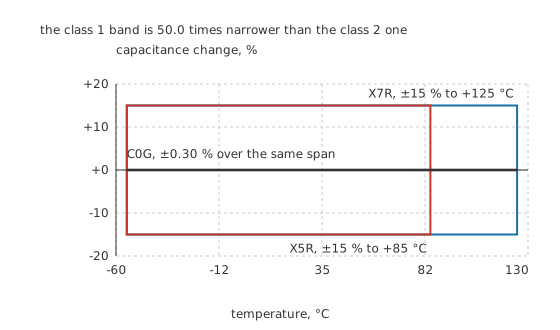
The class 1 band is drawn as a line because at this scale it is one.
That is a band 50.0 times narrower, which is why class 1 parts are what a filter corner or an oscillator load is built from and class 2 parts are what everything else is built from.
The character the code does not have is the important one. Nothing in X5R or X7R says anything about DC bias, and DC bias is a larger effect than temperature by a wide margin.
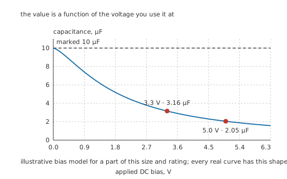
Illustrative bias model for a part of this size and rating. Every real curve has this shape.
The curve is a two-constant stand-in rather than a measurement: a characteristic voltage of 1.9 V and an exponent of 1.4, chosen so the shape matches what a part of this size and rating does. A real datasheet publishes the measured curve, and every one of them falls this way.
Worked example — What a 10 µF part is worth on a 5 V rail
Take a 10 µF class 2 part rated 6.3 V, the ordinary choice for bulk decoupling on a small board.
Sitting on a 5.0 V rail, its capacitance has fallen to 2.05 µF, which is 20.5 % of what the part is marked. On a 3.3 V rail it is 3.16 µF, which is better and still less than a third.
Nothing is wrong with the part. It meets its specification at both points, because its specification never promised anything about bias.
The practical consequence is that a designer who needs a known capacitance on a rail either uses a part rated far above the working voltage, which costs package size, or uses class 1, which costs capacitance, or measures the effective value at the working point and designs around it.
Engineer
Where the capacitance comes from, and what it costs
Hundreds of capacitors in one brick
A multilayer ceramic capacitor is not one capacitor. It is a stack of metal electrodes interleaved from alternate ends, separated by fired ceramic, all in parallel.
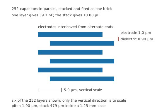
Only the vertical direction is to scale. Each layer gives 39.7 nF and 252 of them give 10.00 µF.
One layer of 1.26 square millimetres in a ceramic of relative permittivity 3.2 k, separated by 0.90 µm in a vacuum permittivity of 8.854 pF/m, gives 39.7 nF. Put 252 of them in parallel and the total is 10.00 µF. With 1.0 µm of electrode between dielectric layers the pitch is 1.90 µm, so the active stack stands 479 µm tall and fits inside a 1.25 mm case with room for cover layers at each end.
Both terms in that calculation are being pushed hard. The permittivity is in the thousands rather than the low single figures a plastic film offers, and the layer is under a micrometre thick. The first is what makes the part class 2, and the second is what makes it fragile.
Why the high permittivity comes with strings attached
The materials that reach permittivities in the thousands are ferroelectric: their crystal structure has a built-in electrical polarity that can be flipped by an applied field, and it is the flipping that gives the enormous apparent capacitance. That mechanism explains all three of class 2's inconveniences at once.
Bias. Once the field has aligned most of the domains, there are fewer left to align, so the incremental capacitance falls. That is the sponge, and it is fully reversible.
Temperature. The material has a transition temperature above which the ferroelectric behaviour disappears, and the permittivity peaks near it. So the value moves substantially with temperature and does so in a curve rather than a straight line, which is why the specification is a band rather than a coefficient.
Ageing. After the part is fired and cooled through that transition, the domain structure keeps settling for years. The capacitance falls roughly by a fixed percentage per decade of elapsed hours, so most of the loss happens in the first weeks and it never quite stops. Heating a part above its transition temperature, which soldering does, resets the clock, so a freshly soldered board measures higher than the same board a month later.
Class 1 dielectrics are not ferroelectric. They get their permittivity from ordinary electronic polarisation, which is small, linear, almost temperature-independent and does not age. Everything good about C0G and everything limiting about it come from that one fact. Dielectrics covers the material physics behind both.
Professional
What is actually left, and what else the package costs
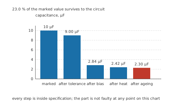
Every step is inside specification. The part is not faulty at any point on this chart.
The deratings are independent and they multiply. Start at the marked 10 µF. A 10 % tolerance takes the worst case to 9.00 µF. Working at 3.3 V takes it to 2.84 µF. A hot enclosure costs another 15 %, giving 2.42 µF, and an illustrative 5.0 % of ageing gives 2.30 µF. What arrives at the circuit is 23.0 % of what is printed on the part.
Designers who know this fit two or three times the nominal capacitance they calculated, or specify the effective value at the operating point rather than the marked one. Designers who do not know it ship a product that works on the bench and misbehaves in a warm cabinet eighteen months later.
The package trades, all inside one outline
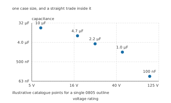
Same volume, divided between thinner layers for capacitance or thicker ones for rating.
Within a case size, capacitance and voltage rating trade directly, because both come from the layer thickness. That is why the answer to bias loss is rarely "the same part rated higher in the same package": the higher-rated part starts with less capacitance, and the two effects partly cancel. Going up a case size is usually the real answer, and it is the one that costs board area.
Three more things the package brings
Cracking. A ceramic brick soldered rigidly to a board that flexes is a ceramic brick under bending stress. Board flexure during depanelling, connector insertion or a drop puts cracks through the stack, and a crack that shorts two electrodes shorts the rail. It is a leading cause of field failures on assembled boards and the reason larger case sizes are avoided near board edges and mounting holes. Failure modes covers what the crack does next.
Microphonics. A ferroelectric material is also piezoelectric, so a class 2 capacitor changes shape slightly with applied voltage and generates a voltage when it is squeezed. On a board carrying audio-frequency ripple, that turns capacitors into small loudspeakers, which is the singing that some switching supplies do. Run the mechanism the other way and vibration injects noise into a sensitive node. Class 1 parts do neither.
No polarity, and very low ESR. Ceramics are not polarised and their series resistance is the lowest of any family, which is why they are the default for high-frequency decoupling. That very low resistance is not always a gift: it removes damping, and a ceramic bank on the input of a converter can ring hard with the inductance of the wiring feeding it. ESR and parasitics treats that properly.
The selection rule that comes out of all this is short. If the value matters, use class 1 and accept the capacitance you can get. If the value does not matter and the job is to be a low impedance, use class 2, fit more than you calculated, and check the bias curve for the voltage you are actually running at. Choosing the right capacitor puts that beside the other families.
Common mistakes
- Reading the marked value as the working value — a class 2 part on a rail near its rating can deliver a quarter of what is printed on it, and it is inside specification while it does.
- Treating X7R and C0G as interchangeable because both say "ceramic" — one holds its value to a fraction of a percent and the other does not hold it at all. For a filter corner or an oscillator load, only class 1 will do.
- Assuming the temperature code covers bias — it does not. The three characters describe temperature only, and bias is the larger effect.
- Fitting a large case size near a board edge or a mounting hole — ceramic cracks under board flexure, and a cracked stack usually fails as a short across whatever it was decoupling.
- Measuring a freshly soldered board and trusting the number — soldering resets class 2 ageing, so the same board reads lower weeks later without anything having gone wrong.
Frequently asked questions
What is the difference between class 1 and class 2 ceramic capacitors?
The dielectric material. Class 1, such as C0G, uses a linear dielectric with a low permittivity: the value is stable across temperature, bias and time, and the capacitance per package is small. Class 2, such as X5R and X7R, uses a ferroelectric dielectric with a permittivity in the thousands, which buys far more capacitance and gives back a large part of it under working conditions.
Why does my 10 µF ceramic measure much less in circuit?
Because of DC bias. A class 2 dielectric loses capacitance as the applied voltage rises, and on a rail near the part's rating the loss can be most of the value. The part recovers fully when the voltage is removed, which is why it measures correctly on a bench meter with no bias applied.
What does X7R mean?
It is specified from −55 °C to +125 °C, and across that span its capacitance may change by up to fifteen percent either way. The first character is the low temperature, the second the high one, and the third the permitted change. The code says nothing about DC bias, tolerance or ageing.
Do ceramic capacitors age?
Class 2 ones do. After firing, the dielectric's domain structure keeps settling, and the capacitance falls by a few percent per decade of elapsed hours. Most of it happens early. Heating the part above its transition temperature, which reflow soldering does, resets the process. Class 1 parts do not age this way.
Why do some circuit boards make a high-pitched noise?
Class 2 ceramic dielectrics are piezoelectric as well as ferroelectric, so they change shape slightly with applied voltage. A capacitor carrying ripple at an audible frequency flexes the board it is soldered to, and the board radiates it. Class 1 parts and film capacitors do not do this.