
Quick Answer
A switching regulator chops its input into pulses and lets an inductor and a capacitor average them back into a steady voltage. The switch is either fully on or fully off, never both carrying current and holding voltage, so it wastes almost nothing. The output is the input times the fraction of time it is closed.
Intuition
Never held halfway
Holding a door ajar is work. Your arm has to keep pushing against the closer, and it goes on being work for as long as the door stays where you put it. Let the door swing fully open against its stop, or let it latch fully shut, and the effort stops entirely. Nothing about the door changed. What changed is that it is no longer being held between two positions.
A linear regulator is a door held ajar. Its pass element sits partly conducting, with volts across it while amps flow through it, and the product of those two is heat for as long as the circuit is powered. It is not doing anything wrong; it is doing exactly what holding something part-way costs.
A switch is never held part-way. When it is off, no current flows, so nothing is dissipated. When it is on, there is almost no voltage across it, so almost nothing is dissipated. Either state is nearly free, and the only expensive part of a switch's life is the instant it spends travelling between them.
That is the whole idea. Chop the input into pulses, smooth them back into a steady voltage with an inductor and a capacitor, and the difference between input and output stops being heat and starts being time.
This lesson stays on the bench. Everything below runs from a 12 V supply to a 3.3 V output. Converters that work directly from the mains are a different subject with different hazards, and none of them appears here.
Practitioner
Four parts, and the node between them
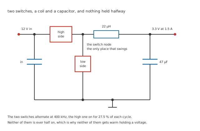
Five junction dots and no crossings. The switch node is the only place in the circuit that swings.
An invented synchronous buck converter carries this lesson: 12 V in, 3.3 V out, 1.5 A of load, 400 kHz of switching, 22 µH and 47 µF. Every number attached to it is an invention.
Two switches in series between the supply and ground take turns. Their meeting point — the switch node — is therefore a square wave between the full input and ground, and it is the only node in the circuit with any large signal on it. Everything downstream of the inductor is meant to be steady.
Worked example — What the duty ratio buys
The switch node spends a fraction of each cycle at 12 V and the rest at zero, so its average is the input times that fraction.
To average 3.3 V the fraction must be 0.275, or 27.5 %.
At 400 kHz the period is 2.50 µs, so the high side conducts for 688 ns and the low side for 1.81 µs.
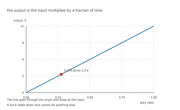
The line goes through the origin and stops at the input.
That straight line is also the arrangement's limit. Everything a buck can produce lies on it, so it steps down and cannot step up — a fact worth holding on to, because the other arrangements exist precisely to escape it.
Engineer
What the inductor and the capacitor each do
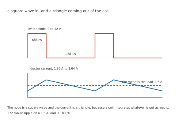
The current's mean sits exactly on the 1.5 A the load takes.
The inductor is not a filter in the way a resistor and capacitor make a filter. It is a current source with inertia: put a voltage across it and the current through it ramps, and the steeper the voltage the steeper the ramp.
Worked example — The ripple the coil allows
While the high side conducts, the inductor has 8.7 V across it — input minus output — for 688 ns.
22 µH under that voltage for that long ramps by 272 mA, which is 18.1 % of the load.
So the current swings between 1.36 A and 1.64 A and averages the 1.5 A the load actually takes. Then the low side conducts, the inductor sees minus 3.3 V, and the ramp reverses.
The capacitor's job is what is left over. The inductor already supplies the load continuously; the capacitor absorbs only the triangle riding on top of it.
Worked example — And the ripple the capacitor allows
Half the triangle is above the mean and half below, and the capacitor takes that difference in and gives it back twice per cycle.
47 µF handling 272 mA at 400 kHz gives 1.81 mV of output ripple, or 0.0548 % of the rail.
Treat the capacitor as a reservoir supplying the whole load between refills instead — which is what a rectifier's capacitor does — and the same arithmetic gives 79.8 mV, 44.1 times too much.
That factor of 44.1 is worth stopping on. Both relations are correct about their own circuit and reaching for the wrong one is easy, because both are "ripple on a capacitor". The question that separates them is whether anything else is supplying the load while the capacitor waits. In a rectifier nothing is. Here the inductor is, all the time.
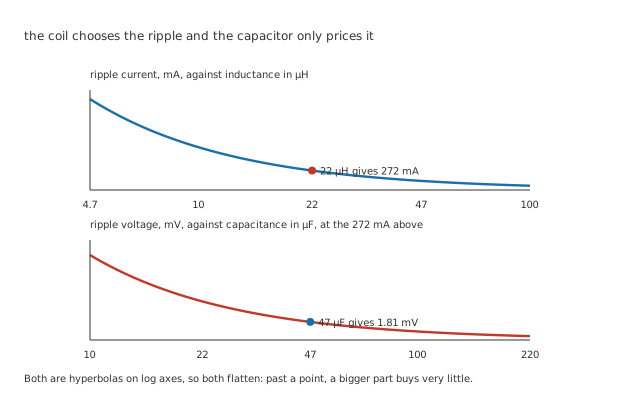
Both hyperbolas flatten, so past a point a bigger part buys very little.
The two panels are not independent, and the order matters. The inductor decides how much ripple current exists at all; the capacitor only decides what that current costs in volts. A designer who is unhappy with the output ripple and reaches for a bigger capacitor is working on the second panel when the first one is usually cheaper.
Professional
What it costs, and what it costs you
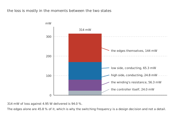
The edges alone are 45.8 % of the total.
"Almost nothing" is not nothing, and the losses that remain have names.
Worked example — Adding up what a switching converter wastes
The edges. Each transition takes 20 ns with both voltage and current partly present, 400 kHz times a second: 144 mW.
Conduction. 40 mΩ carrying 1.5 A costs 24.8 mW in the high side and 65.3 mW in the low side, in proportion to how long each conducts.
The winding. 25 mΩ of copper adds 56.3 mW. The controller draws 2.0 mA for itself, or 24.0 mW.
Together 314 mW against 4.95 W delivered: 94.0 %.
Notice which term is largest. 45.8 % of the loss is in the transitions, and that term is the only one proportional to the switching frequency. Halve the frequency and it halves — at the cost of a bigger inductor for the same ripple, because the on-time doubles. That trade is the central decision in every switching design, and it is why converters do not simply run as fast as possible.
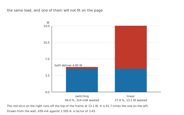
The red slice on the right runs off the page, and that is the honest way to draw it.
Worked example — The same job, done the other way
A linear regulator taking the same 12 V to the same 3.3 V at 1.5 A drops 8.7 V across its pass element, and with 5.0 mA of quiescent current on top it dissipates 13.1 W, at 27.4 %.
That is 41.7 times the switching converter's heat, for the same 4.95 W at the load.
From the supply it draws 1.505 A against 439 mA: a factor of 3.43 on a battery, and the difference between a heatsink and no heatsink.
What you pay instead
Noise. A node swinging 12 V in 20 ns radiates, and every loop carrying that current radiates with it. The output ripple of 1.81 mV is the polite part; the switching harmonics are the part that turns up in an unrelated measurement.
Layout. The loop carrying the chopped current has to be small, and which loop that is depends on the arrangement. A switching converter that works on a breadboard and fails on a board is nearly always a layout problem rather than a component one.
Parts. An inductor, two switches, a controller and more capacitance than a linear part needs, against one three-terminal device and a capacitor.
And complexity in the failure modes. A linear regulator that fails usually gets hot. A switching converter can oscillate, skip pulses, saturate its inductor or fail to start under load, and telling those apart needs an oscilloscope on the switch node.
Which to reach for
Small drop, small current, quiet rail: linear. At a volt of drop and tens of milliamps, the heat is trivial and the noise is the lowest available.
Large drop, or a wide input range, or battery life: switching. 13.1 W against 314 mW is not a trade-off, it is a decision already made.
And often both. A switcher takes a battery or a wall supply down close to the rail, and a small linear regulator cleans up the last volt for whatever cannot tolerate the ripple. The switcher does the work; the linear part does the manners.
Common mistakes
- Sizing the output capacitor with a rectifier's ripple formula — 47 µF gives 1.81 mV here, and the reservoir relation gives 79.8 mV, which is 44.1 times too much. The inductor supplies the load continuously; the capacitor only takes the triangle.
- Reaching for a bigger capacitor to fix ripple — the inductor decides how much ripple current exists. 22 µH is what sets the 272 mA; the capacitor only prices it.
- Assuming a higher switching frequency is better — the edges are 144 mW of a 314 mW total, and that term alone scales with frequency. What a higher frequency buys is a smaller inductor.
- Treating a buck as a general-purpose converter — its output is the input times a fraction of time, so it steps down and only down. Everything it can do lies under that line.
- Ignoring the switch node when laying out — 12 V in 20 ns is the noisiest thing on the board, and the loop it drives is what decides whether the converter is quiet or a radio transmitter.
- Expecting a switching failure to look like a thermal one — a linear regulator in trouble gets hot; a switcher skips pulses, oscillates or refuses to start, and the switch node is the only place any of that is visible.
Frequently asked questions
Where does the energy actually go during the on-time?
Into the inductor's magnetic field and on to the load at the same time. The load draws its current continuously, and while the high side conducts the inductor's current is rising, so it is passing on more than the load takes and storing the surplus. During the off-time the inductor's current falls, it delivers more than is arriving, and the store comes back out. Nothing is thrown away in either half, which is the whole difference from a linear part.
What is the low-side switch for? A diode would do.
It would, and many converters use one. A diode drops several hundred millivolts while conducting, and here that would be conducting for 72.5 % of every cycle at 1.5 A, which is far more than the 65.3 mW a switch costs. Replacing that diode with a second switch is called synchronous rectification, and it is why efficiency figures above about 90 % became ordinary.
Why does ripple current matter if the output ripple is only 1.81 mV?
Because the inductor and the switches carry it. The peak current is 1.64 A rather than 1.5 A, and it is the peak that saturates a core and the peak that a current limit responds to. A design that sizes its inductor from the average current and then runs a large ripple can saturate at a load the arithmetic said was comfortable.
Can this arrangement produce a higher output than its input?
Not this one. A buck's output is the input multiplied by a number between zero and one, so it steps down. Rearranging the same three parts — putting the inductor across the input and switching it to ground — makes a boost converter, which steps up, and there are arrangements that do both or invert. They share the idea and none of them shares the duty-to-output relation, which has to be re-derived for each.
Does the efficiency stay at 94 % across the load range?
No, and this is where a switching converter's headline figure misleads in the same way a linear one's does. The controller's 24.0 mW and most of the 144 mW of edge loss are there whatever the load, so at a tenth of this load they are a much larger share of a much smaller output. Good controllers switch to a pulse-skipping mode at light load precisely to shrink that fixed cost.